• Journal of Semiconductors
  • Vol. 44, Issue 12, 121801 (2023)
Chenglin Du1、2, Ran Ye1、2、*, Xiaolong Cai1、2、**, Xiangyang Duan1、2, Haijun Liu2, Yu Zhang2, Gang Qiu2, and Minhan Mi3
Author Affiliations
  • 1State Key Laboratory of Mobile Network and Mobile Multimedia Technology, Shenzhen 518055, China
  • 2Wireless Product Planning Department, ZTE Corporation, Shenzhen 518055, China
  • 3School of Microelectronics, Xidian University, Xi’an 710071, China
  • show less
    DOI: 10.1088/1674-4926/44/12/121801 Cite this Article
    Chenglin Du, Ran Ye, Xiaolong Cai, Xiangyang Duan, Haijun Liu, Yu Zhang, Gang Qiu, Minhan Mi. A review on GaN HEMTs: nonlinear mechanisms and improvement methods[J]. Journal of Semiconductors, 2023, 44(12): 121801 Copy Citation Text show less
    Relationship between capacitance and voltage for GaN HEMT.
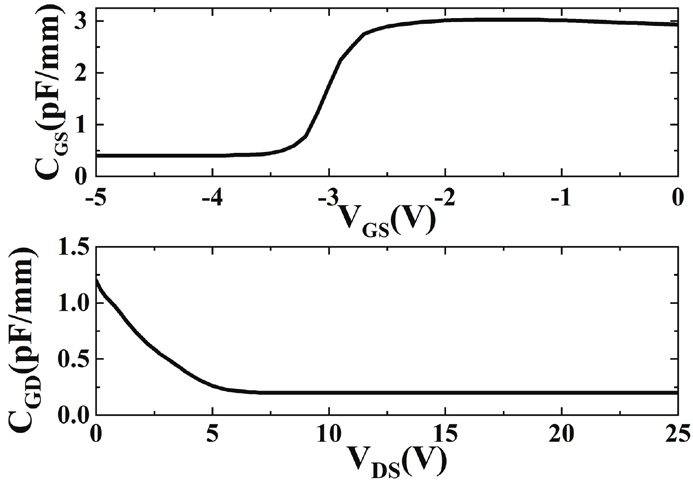
    Fig. 1. Relationship between capacitance and voltage for GaN HEMT.
    (Color online) GaN HEMT: (a) transconductance gm(VGS) curves. (b) Channel transconductance gDS(VDS) curves.
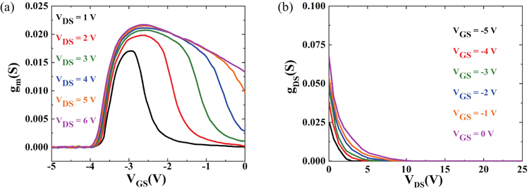
    Fig. 2. (Color online) GaN HEMT: (a) transconductance gm(VGS) curves. (b) Channel transconductance gDS(VDS) curves.
    Parasitic source and drain access resistances of GaN HEMT.
    Fig. 3. Parasitic source and drain access resistances of GaN HEMT.
    Longitudinal electric field at the source access region for different VGS. The simulated increase in rS is plotted in the right axis[41].
    Fig. 4. Longitudinal electric field at the source access region for different VGS. The simulated increase in rS is plotted in the right axis[41].
    AlGaN/GaN HEMT output and transconductance characteristics at VGS = 0 V[47].
    Fig. 5. AlGaN/GaN HEMT output and transconductance characteristics at VGS = 0 V[47].
    (Color online) Pulsed gm versus VGS characteristics for the GaN HEMT with different quiescent bias point[55].
    Fig. 6. (Color online) Pulsed gm versus VGS characteristics for the GaN HEMT with different quiescent bias point[55].
    Frequency dispersion of output current, transconductance at quiescent large signal bias point, and gate capacitance at VDS = 0 V[61].
    Fig. 7. Frequency dispersion of output current, transconductance at quiescent large signal bias point, and gate capacitance at VDS = 0 V[61].
    (Color online) Existing mechanisms of gm reduction for the GaN HEMT.
    Fig. 8. (Color online) Existing mechanisms of gm reduction for the GaN HEMT.
    (Color online) Schematic diagram of gate and source field plate of GaN HEMT.
    Fig. 9. (Color online) Schematic diagram of gate and source field plate of GaN HEMT.
    (Color online) (a) Cross section of AlGaN/GaN HEMTs with Si-rich SiN interlayer. (b) TEM of devices with Si-rich SiN interlayer[84].
    Fig. 10. (Color online) (a) Cross section of AlGaN/GaN HEMTs with Si-rich SiN interlayer. (b) TEM of devices with Si-rich SiN interlayer[84].
    (Color online) Two-tone linearity measurement at 1 GHz with a 1-MHz spacing of the (a) proposed device and (b) conventional device. Devices are biased at VDS = 10 V near class A[85].
    Fig. 11. (Color online) Two-tone linearity measurement at 1 GHz with a 1-MHz spacing of the (a) proposed device and (b) conventional device. Devices are biased at VDS = 10 V near class A[85].
    (Color online) Device structure of nanowire channel HEMT[95].
    Fig. 12. (Color online) Device structure of nanowire channel HEMT[95].
    (Color online) (a) Source resistance as a function of drain current density in planar and nanowire devices. Inset: measurement setup. (b) Transfer characteristics of nanowire channel and planar device[95].
    Fig. 13. (Color online) (a) Source resistance as a function of drain current density in planar and nanowire devices. Inset: measurement setup. (b) Transfer characteristics of nanowire channel and planar device[95].
    (Color online) Schematic illustration of a GaN field-effect transistor with buried dual gates[101].
    Fig. 14. (Color online) Schematic illustration of a GaN field-effect transistor with buried dual gates[101].
    (Color online) (a) Schematics of laterally gated device. (b) OIP3 of planar and laterally gated devices at 3−4 GHz range[102].
    Fig. 15. (Color online) (a) Schematics of laterally gated device. (b) OIP3 of planar and laterally gated devices at 3−4 GHz range[102].
    (Color online) (a) Diagram of the super-lattice castellated FET structure combining a super-lattice epitaxial channel with a three-dimensional, castellated T-gate. (b) Two-tone linearity measurement at 30 GHz[103].
    Fig. 16. (Color online) (a) Diagram of the super-lattice castellated FET structure combining a super-lattice epitaxial channel with a three-dimensional, castellated T-gate. (b) Two-tone linearity measurement at 30 GHz[103].
    (Color online) Schematic of planar nanostrip GaN HEMT[105].
    Fig. 17. (Color online) Schematic of planar nanostrip GaN HEMT[105].
    (Color online) (a) Schematic cross section of AlGaN/GaN PolFET with graded heterostructure. (b) Top: energy-band profiles. Bottom: electron distributions. Inset: schematic cross section of PolFETs and HEMTs structures[107].
    Fig. 18. (Color online) (a) Schematic cross section of AlGaN/GaN PolFET with graded heterostructure. (b) Top: energy-band profiles. Bottom: electron distributions. Inset: schematic cross section of PolFETs and HEMTs structures[107].
    (Color online) (a) Schematic diagram for the MOCVD-grown HEMT with a graded InGaN subchannel. (b) Two-tone linearity measurements with f1 = 10 GHz and f2 = 10.01 GHz biased near Class A[111].
    Fig. 19. (Color online) (a) Schematic diagram for the MOCVD-grown HEMT with a graded InGaN subchannel. (b) Two-tone linearity measurements with f1 = 10 GHz and f2 = 10.01 GHz biased near Class A[111].
    (Color online) Cross-sectional schematic of the double-channel HEMT on the GaN on high-resistivity silicon[117].
    Fig. 20. (Color online) Cross-sectional schematic of the double-channel HEMT on the GaN on high-resistivity silicon[117].
    (Color online) Illustration of device-level gm-compensation-g′′m for a set of five independent transistors with slight (0.2−0.3 V) offsets in threshold voltage (left). When these transistors are connected together (right), the composite g′′m (black curve) is lowered[30].
    Fig. 21. (Color online) Illustration of device-level gm-compensation-gm for a set of five independent transistors with slight (0.2−0.3 V) offsets in threshold voltage (left). When these transistors are connected together (right), the composite gm (black curve) is lowered[30].
    (Color online) Schematic and SEM image of the fin device. The widths of the five fin devices are all present within the single fin device[30].
    Fig. 22. (Color online) Schematic and SEM image of the fin device. The widths of the five fin devices are all present within the single fin device[30].
    (Color online) Top-view SEM images of the fabricated device showing a planar region and a fin region under a single gate electrode[120].
    Fig. 23. (Color online) Top-view SEM images of the fabricated device showing a planar region and a fin region under a single gate electrode[120].
    (Color online) (a) TRG-HEMT structure diagram. (b) Cross section view of the TRG-HEMT along the gate width. (c) Cross section view of the TRG-HEMT along the gate length[122].
    Fig. 24. (Color online) (a) TRG-HEMT structure diagram. (b) Cross section view of the TRG-HEMT along the gate width. (c) Cross section view of the TRG-HEMT along the gate length[122].
    (Color online) Transfer characteristics of the AlGaN/GaN MIS-HEMTs with 20 nm SiN and 60 nm PZT at VDS = 10 V[123].
    Fig. 25. (Color online) Transfer characteristics of the AlGaN/GaN MIS-HEMTs with 20 nm SiN and 60 nm PZT at VDS = 10 V[123].
    (Color online) Schematic cross section of the AlGaN/GaN HEMT with a dual-gate structure[129].
    Fig. 26. (Color online) Schematic cross section of the AlGaN/GaN HEMT with a dual-gate structure[129].
    (Color online) Cross-sectional view of dual gate ferroelectric GaN HEMT[130].
    Fig. 27. (Color online) Cross-sectional view of dual gate ferroelectric GaN HEMT[130].
    (Color online) Reported GVS and peak gm of recent improvement methods for the GaN HEMT.
    Fig. 28. (Color online) Reported GVS and peak gm of recent improvement methods for the GaN HEMT.
    (Color online) Reported results of two-tone linearity measurement of recent improvement methods for the GaN HEMT.
    Fig. 29. (Color online) Reported results of two-tone linearity measurement of recent improvement methods for the GaN HEMT.
    TypesMechanismsChallenges
    Trapping suppressionReduce the electric field;eliminate the sources of the traps;keep the 2DEG from the trapsMostly have no ability to further improvethe GVS
    Nanowire channel (fin structure/tri-gate)Effectively suppress the increasing of rS due to the large current drivabilityExtra parasitic gate capacitance;loss of the output current;etching damage risk
    Graded channel (PolFET with 3DEG)Maintain the stable electron volume to suppress scatteringLow peak gm;complex epitaxy process of the graded channel
    Double channelReduce perpendicular electric field;electron compensation between double channelMultiple epitaxy of the double channel
    gm compensationDifferent gm compensated with each otherPrecise design for threshold voltage;hard process control for stable threshold
    Ferroelectric dielectric/N-polar hetero-structureNonlinear polarization effect of PZT / improvement of electron confinementTough epitaxy growth of N-polar
    Double gateAlleviate the electric fieldLow peak gm
    Table 1. Features of reported improvement methods for nonlinear gm.
    Chenglin Du, Ran Ye, Xiaolong Cai, Xiangyang Duan, Haijun Liu, Yu Zhang, Gang Qiu, Minhan Mi. A review on GaN HEMTs: nonlinear mechanisms and improvement methods[J]. Journal of Semiconductors, 2023, 44(12): 121801
    Download Citation