Chenglin Du, Ran Ye, Xiaolong Cai, Xiangyang Duan, Haijun Liu, Yu Zhang, Gang Qiu, Minhan Mi. A review on GaN HEMTs: nonlinear mechanisms and improvement methods[J]. Journal of Semiconductors, 2023, 44(12): 121801
Copy Citation Text
The GaN HEMT is a potential candidate for RF applications due to the high frequency and large power handling capability. To ensure the quality of the communication signal, linearity is a key parameter during the system design. However, the GaN HEMT usually suffers from the nonlinearity problems induced by the nonlinear parasitic capacitance, transconductance, channel transconductance etc. Among them, the transconductance reduction is the main contributor for the nonlinearity and is mostly attributed to the scattering effect, the increasing resistance of access region, the self-heating effect and the trapping effects. Based on the mechanisms, device-level improvement methods of transconductance including the trapping suppression, the nanowire channel, the graded channel, the double channel, the transconductance compensation and the new material structures have been proposed recently. The features of each method are reviewed and compared to provide an overview perspective on the linearity of the GaN HEMT at the device level.
Gallium nitride (GaN) is regarded as an extremely potential material for high power applications due to its wide band gap and high breakdown field[1−3]. A high electron mobility transistor (HEMT) is popular for high-frequency applications because of its high-density two dimensional electron gas (2DEG) originated from the GaN-based hetero-junction[4−7]. With the development of the wireless communication system, the network needs to offer a greater data transfer rate, lower transmission delay and higher signal quality, which requires high-performance electronic devices[8, 9]. Nowadays, more and more GaN HEMTs are employed into radio frequency (RF) front ends to replace conventional silicon-based devices due to their excellent properties[10−12].
In the RF front ends, to ensure the quality of communication, linearity is a key parameter in system design. Nonlinearity problems result in significant side bands, saturation of output power at high input powers, an increase of error vector magnitude and further deteriorates the transmission quality of signal[13−15]. Thus, many circuit-level methods have been proposed to overcome this nonlinearity problem including the back-off, the feed-forward, the feedback, the digital pre-distortion, etc.[16−21]. However, as the operation frequency increases gradually to cater to high data capacity, the implementation of circuit-level linearization turns out to be more and more complex and high-cost. As a core device in the RF front ends, a direct improvement of linearity upon the GaN HEMT is one of effective and low-cost methods to suppress the nonlinearity problem in the system.
Over the past decade, the GaN HEMT was widely applied in the commercial wireless communication field due to its superior performance[22−24]. With the massive deployment of the GaN HEMT, the linearity issue attracts more and more attention. Plenty of investigations on the device linearity improvement for the GaN HEMT have emerged for more competitive device performances, such as modification, optimization or innovation of the device structure and fabrication process. In order to provide an overview perspective on the GaN HEMT that serves as references for high linearity and high-performance devices in the future, in this review, we summarize the main nonlinear sources in the GaN HEMT. Then, the physical mechanisms of nonlinearity, especially transconductance, at the device level are discussed and analyzed for the GaN HEMTs. At the end, according to these mechanisms, many device-level improvement methods in recent years are reviewed and discussed.
Nonlinear sources of GaN HEMTs
The fifth-generation (5G) wireless communication system needs high signal transmission quality to satisfy the low transmission delay. In practical system applications, if the linearity of the power amplifier (PA) is poor, the signal is susceptible to interference from adjacent channels, resulting in a high bit error rate. The system has to transmit the signal several times to improve communication quality and then the transmission delay increases. Thus, it requires very stringent linearity for PAs in the RF front ends[25]. The nonlinearity of PAs is usually characterized by the intermodulation distortion (IMD), the amplitude modulation to amplitude modulation (AM/AM) distortion and the amplitude modulation to phase modulation (AM/PM) distortion.
One obvious property of a nonlinear system is its harmonics generation of the excitation frequency or frequencies. The intermodulation products are mixture components with different frequencies generated from nonlinear device elements. When two input signals with ω1 and ω2 are applied to the input terminal of the PA, besides the fundamental signal at a ω1 and ω2, the output signal also contains many mixed harmonics due to the nonlinear effect. Because the third-order intermodulation (IMD3) products at 2ω1−ω2 and 2ω2−ω1 are close to the fundamental frequency and difficult to filter, usually, the IMD3 attracts more attention than others.
The AM/AM distortion is a nonlinear power relationship between input signal and output signal. With the input power increasing, the output power no longer increases linearly. As a result, the AM to AM conversion is not kept as a constant. Similarly, the AM/PM distortion is a phenomenon wherein changes in the amplitude of a signal applied to a nonlinear circuit cause a phase shift. This distortion can lead to serious consequences if it occurs in a system in which the signal’s phase is important.
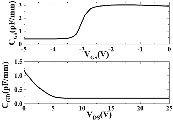
Based on the Volterra Series analysis, the nonlinearity mainly comes from the transconductance (gm), the channel transconductance (gDS), the gate-to-source capacitance (CGS) and the gate-to-drain capacitance (CGD)[26, 27]. The top picture of Fig. 1 shows the nonlinear variation of CGS versus gate-to-source voltage (VGS). Due to the existence of 2DEG, CGS decreases rapidly near the pinch-off voltage. Likewise, the variation of CGD versus the drain-to-source voltage (VDS) is displayed in the bottom picture of Fig. 1 and it is also nonlinear with VDS. Owing to these variations, the capacitances have nonlinear impacts on the linearity of RF PAs. It is reported that a growing significance of CGS induced the IMD role when the frequency increases in the microwave region and certain bias shifts of the mentioned sweet spot[28]. According to the expression of physical model analyzed in Ref. [13], both CGS and CGD can lead to the AM/AM and AM/PM distortion. Especially in the GaN based PAs, the AM/PM distortion is contributed by the input impedance variation due to the nonlinear CGS and CGD[29].
Figure 1.Relationship between capacitance and voltage for GaN HEMT.
Fig. 2 shows the gm and gDS curves as the function of VGS and VDS, respectively. In a certain range of VGS and VDS, the values of gm and gDS change nonlinearly. However, the nonlinear change of gm is worse and the linear region of gm is narrower. According to Eqs. (1) and (2), the harmonics vO2 and vO3 are proportional to the first derivative of gm () and the second derivative of gm ()[30]. The output third-order intercept power (OIP3) is related to the gm and according to Eq. (3)[31].
Except for the above sources, the bias condition, the source/load impedance, the operation frequency, the gate leakage current, the drain-to-source capacitance are possible to lead to the nonlinearity of the GaN HEMT[31−33]. However, as for the GaN HEMT, the parasitic capacitance is usually small and the other nonlinear effects are relatively not obvious. Generally, the transconductance (gm) is considered as the most main nonlinearity contributor in the GaN HEMT[31, 32]. Therefore, we mainly focus on the physical mechanism of the nonlinear gm for the GaN HEMT in detail.
Physical mechanisms of nonlinear transconductance
To conveniently describe the gm profile or the gm flatness, a gate voltage swing (GVS), which is a gate voltage range that has at least its 80% peak gm value, is defined as a figure of merit to indicate the linearity at the device level[34]. In this way, if the wider GVS is, the lower values of and will be, meaning that the harmonic outputs are suppressed. In order to achieve the wider GVS, the physical mechanisms of that gm reduced with the gate voltage are discussed in many works.
Scattering effect
The sheet concentration of 2DEG ns is changed by the gate easily because the 2DEG is distributed in a narrow range of the hetero-interface. As the gate voltage increases, the electron concentration rises rapidly and the electron mobility and velocity reduces due to the scattering effect. The longitudinal optical phonon is found to be responsible for the electron velocity reduction, further causing the drift velocity to saturate, particularly in the place where high sheet carrier densities exist due to the hot phonon effect[35, 36]. Fang et al.[37] also took the effect of optical phonon scattering on the electron velocity into consideration. It is demonstrated that the saturation current is proportional to at high carrier concentration, and the gm will decrease as gm = ~1/. Bajaj et al.[38] successfully calibrated the transport model, including the effect of optical phonon scattering on electron velocity by the direct sheet density measurement.
In addition, the interface roughness scattering is responsible for the reduction of the electron mobility and velocity. Juang et al.[39] reported that the electron wave function is pressed closely against the AlGaN/GaN hetero-interface in the high electron concentration state, which causes the electron mobility to drop off due to the interface roughness scattering. Especially, the effect of interface roughness scattering is more serious with the high gate voltage that induces the high electron concentration. Li et al.[40] demonstrated that the high perpendicular electric field generated by gate voltage aggravates the interface roughness scattering and degrades the electron velocity. With the increasing gate voltage, the electron velocity begins to reduce. This is expected since the changes of the gate voltage primarily affect the interface scattering while the other processes are only mildly changed.
Access resistance
To ensure the high-power handling capability, the source and drain regions of GaN HEMT are not self-aligned with the gate electrode. However, the non-self-aligned structure brings in extra parasitic access resistance in the source and drain regions, as shown in Fig. 3. Palacios et al.[41] demonstrated that the increasing of dynamic source access resistance (rS) is the main reason for the gm reduction. With the increasing gate voltage, the electric field is higher than 10 kV/cm. At this electric field, the electron velocity has already started its “quasi-saturation” which produces a decrease in the electron mobility, along with the increasing rS (see Fig. 4)[42, 43].
Figure 3.Parasitic source and drain access resistances of GaN HEMT.
Trew et al.[44] reported that the increasing rS is attributed to the space charge limitation under the high current state. Under this condition, the injected charges in the semiconductor become comparable in magnitude to the background impurity density when the device stays under large-signal RF operation. Once space charge limitation is established, the resistivity increases rapidly with the current and the distance from the source injection point. In this way, the rS expression is formed in Eq. (4), where rSS denotes the low current magnitude of the resistance in the gate−source region, ΔrSS denotes the increased resistance due to the space charge limitation, ISC denotes the space charge threshold current. Except for the space charge limitation effect, the polarization coulomb field (PCF) scattering is discussed as one reason for the increasing rS with a longer gate length or a shorter gate-source distance by Yang et al.[45].
The drain access resistance (rD) is also taken into account for the gm reduction according to Chen et al.[46]. The high rD pushes the device from the saturation state to the linear state, which causes the gm reduction. Considering the gate-controlled voltage is closely related to the value of rS, the dynamic change of rS attracts more attention according to the reported studies. However, the dynamic change of rD also needs attention due to its negative effect.
Self-heating effect
The self-heating effect is common in the Si device when it operates at a high power state. In the GaN HEMT, the self-heating effect on gm is investigated by Kuzmik et al.[47]. As expected with Si, if the device temperature is raised, the low-field electron mobility in the channel decreases, and the channel resistance related to the rS increases. As a result, the gm and drain saturation current (Isat) are dispersed with the increasing drain voltage. It is noted that, in Fig. 5, the gm dispersion of the sapphire substrate with worse heat dissipation rate is more steep. The ΔIsat is defined as a difference Isat−, where Isat is a value in a particular HEMT working point and denounced a reference value of the channel at room temperature ( is obtained by extrapolating Isat to VDS = 0 V). Chen et al.[46] further discussed that, with the increasing drain voltage and gate voltage, the transfer and gm curves are easier to be pushed into the region affected by the self-heating, and then they begin to decrease.
Figure 5.AlGaN/GaN HEMT output and transconductance characteristics at VGS = 0 V[47].
Due to the tough growth of GaN-based material, such as dislocations, dangling bonds, vacancies are inevitably brought in the GaN HEMT, which will become the latent sources of traps. The influences of trapping effects on the GaN HEMT usually present as the gate-lag, the drain-lag, the current collapse, the frequency dispersion etc.[48−53]. Specifically, the gate-lag and the drain-lag are transient responses of the drain current under the transient stress[54]. During the stress period, electrons are captured by traps and they have not enough time to de-trap after the stress period due to the long time constant. In this way, the drain current is lower than normal and gradually recovers with time. The current collapse is measured under the condition that the gate and drain are pulsed from the quiescent bias point (VGS,Q & VDS,Q), usually based on the practical operation state, to a voltage respectively. On account of the gate-lag and the drain-lag, the drain current of IDS−VDS characteristic turns to collapse and slump accordingly. As shown in Fig. 6, the gm reduces obviously with different quiescent bias points under the pulse measurement. Besides, a threshold voltage drift towards the positive voltage direction is also observed, which is mainly affected by the gate quiescent bias stress. This effect indicates that traps are present at the interface between the gate and the AlGaN layer, and can effectively change the threshold voltage. Therefore, once these traps are charged by a negative gate voltage pulse, a shift of the gm curve with respect to the (0 V, 0 V) bias point is obtained[55].
Figure 6.(Color online) Pulsed gm versus VGS characteristics for the GaN HEMT with different quiescent bias point[55].
For the GaN HEMT, the traps were reported in the AlGaN barrier, the AlGaN surface and the GaN buffer. The trapping behaviors usually occur in the region with a high electric field, typically in the gate−drain access region[56, 57]. Meneghesso et al.[58] demonstrated that when a high drain−gate bias is applied to the device, electrons may tunnel from the gate toward surface states located within the gate−drain access region: The accumulation of negative charge acts as a virtual gate at the surface of the HEMT, and induces an increase of the channel resistance, and a decrease of the peak gm. Du et al.[59] found that the acceptor-like traps in the barrier layer under the gate is the main cause of nonlinear gm behavior. When a high drain voltage applied on the device which is doped with C/Fe to improve resistivity, the traps in the buffer capture the electrons in the 2DEG and induce a serious drain current collapse, further causing the gm reduction[55, 60]. Furthermore, due to the different time constant of the traps, the frequency response is not alike. Kohn et al.[61] reported that, with the increasing frequency of the transconductance, the gate capacitance and the output current of the GaN HEMT, a compression tendency exists (see Fig. 7). Based on the results, it can be demonstrated that the trapping effects are the reasons for the gm nonlinearity.
Figure 7.Frequency dispersion of output current, transconductance at quiescent large signal bias point, and gate capacitance at VDS = 0 V[61].
According to the discussions above, there are three main causes that reduce gm in the channel region, including the scattering effect, the self-heating effect and the trapping effects. Due to the scattering effect, the high electric field and the high electron concentration induced by the increasing gate voltage reduce the electron velocity or mobility. As for the self-heating effect, the electron mobility is decreased with the increasing channel temperature and gm reduces as a result. With the change of the gate voltage, the traps under the gate trap or de-trap the electrons and increase the channel resistivity when trapping effects begin to work.
Except for the intrinsic gm of the GaN HEMT, the effect of the access region on the gm reduction is attributed to the other causes. The increasing rS results from the electron mobility reduction induced by high electric field, the electron mobility reduction induced by PCF scattering and the resistivity rise induced by the space charge limitation. In the drain access region, the trapping is one reason for the resistivity increase due to the large electric field. The increasing rD has also an impact on the gm reduction. Usually, to deal with higher voltage, the device is equipped with the large drain access region that increases rD. If rD is large, the operation state of the GaN HEMT will be pushed easier into linear region with the increasing gate voltage and gm reduces as a consequence. The mechanisms of nonlinear gm are reviewed in Fig. 8 to show an overview for the different regions in the GaN HEMT.
Figure 8.(Color online) Existing mechanisms of gm reduction for the GaN HEMT.
Differing from the circuit-level linearization techniques, the improvement at the device level has more benefits, such as the low complexity, the low cost and the easy realization. In light of the aforementioned problems, plenty of device-level methods were proposed to suppress the nonlinear problems.
The improvement methods for the nonlinear capacitance are relatively few. For example, Xue et al.[62] added a gate diode to compensate the nonlinear CGS for the GaN HEMT. Bothe et al.[63] designed a new sunken source field plate to reduce CGS and CGD by 15% and 60% respectively. More device-level methods concentrate on the improvements of gm flatness to achieve a large GVS. Previously, many simple methods were proposed to improve the gm flatness, such as the field plate reducing the channel electric field[64], the self-aligned source and drain eliminating the access resistance[65, 66], the optimization of some structure parameters[67, 68]. However, the effect of these methods seems to be not satisfied with the current requirements. Recently, many novel device-level methods surged to achieve better effects.
Suppression of trapping effects
As one main source of gm reduction, the suppression methods of the trapping effects are discussed first. According to the trap positions, plenty of effective methods of suppressing the trapping effects were proposed. The application of the gate/source field plate reduces the surface electric field and further decreases the electron tunneling possibility through the gate. As a result, gate/source field plate is useful to reduce the trapping risk from the surface traps in the drain access region (see Fig. 9)[57, 69–71].
Figure 9.(Color online) Schematic diagram of gate and source field plate of GaN HEMT.
Surface passivation is a method that directly eliminates the surface dangling bonds and improves the surface chemical stability, which reduces the density of surface traps. The SiNx deposited by metal-organic chemical vapor deposition (MOCVD), or plasma-enhanced chemical vapor deposition (PECVD) is one of the most used passivation materials[72–74]. Although many novel passivation materials were still reported to obtain better performance, such as MgO, ScO3 Al2O3, AlN, MgF2, and TiO2[75–80]. However, the passivation deposition process is negative for the device features, such as the degradation of the leakage current, the breakdown voltage and the high-frequency characteristics[81–83]. Recently, multi-layer passivation became a new method to handle these problems. Liu et al.[84] developed a bilayer Si-rich SiN/Si3N4 passivation which has the ability to reduce the gate leakage current and suppressing current collapse (see Fig. 10). Jing et al.[85] proposed a hybrid PECVD-SiNx/PECVD-SiO2 passivation layer for the GaN HEMT. The SiO2 is used to suppressing the surface traps in the drain access while the SiNx is used to modulate the charge and electric field in the source access region. As seen in the results in Fig. 11, besides the suppression of trapping effects, a 2.84 dB improvement of OIP3/PDC is obtained due to the PECVD-SiNx in the source access region when compared to the conventional one.
Figure 10.(Color online) (a) Cross section of AlGaN/GaN HEMTs with Si-rich SiN interlayer. (b) TEM of devices with Si-rich SiN interlayer[84].
Figure 11.(Color online) Two-tone linearity measurement at 1 GHz with a 1-MHz spacing of the (a) proposed device and (b) conventional device. Devices are biased at VDS = 10 V near class A[85].
Except for the surface passivation, a GaN cap layer is another method to reduce the surface traps. The thin GaN layer is considered to compensate the negative polarization charge or to protect the 2DEG from the surface states[86–89]. The traps in the buffer are more difficult to directly eliminate during the device fabrication because the buffer is sandwiched between the substrate and the barrier layers. In consideration of the source of buffer traps, it requires a sophisticated control of native defects and unintentional dopants during the epitaxy of material[90]. Meanwhile, several novel epitaxial structures were proposed. A buffer-free structure is proposed to suppress the buffer-induced trapping effects. Compared with the conventional Fe-doped buffer, the structure allows for a thin 250 nm-thick unintentional doped GaN layer grown between an AlGaN barrier layer and an AlN nucleation layer[91]. Yao et al.[92] demonstrated that, by inserting a graded AlGaN back-barrier between the GaN channel and the AlGaN buffer layer, the trapping in the buffer induced by the hot-electron effect is effectively blocked, which contributes to a remarkable suppression of the current collapse in the GaN HEMT. It is well known that the growth quality of the GaN buffer is better in the homo-epitaxial GaN substrate. Then, a GaN-on-GaN substrate with an acceptable cost was proposed recently[93]. In a word, the trapping effects are hot and complex issues in the GaN HEMT. Except for the above-mentioned suppression methods, other diverse methods are summarized in our previous work in detail[94].
Although, the gm reduction induced by the trapping effects is suppressed by the aforementioned methods. However, the gm flatness cannot be improved further. Therefore, several novel methods for improving the GVS are introduced as follows.
Nanowire channel
According to the above-mentioned mechanisms, the increasing rS is considered as one reason for the gm roll-off. Lee et al.[95] proposed a kind of nanowire channel HEMT structure aiming to suppress the increase of rS. As shown in Fig. 12, the channel is surrounded with a gate electrode, which bears a close resemblance to the silicon-based fin field-effect transistor (FET)[96], so it is also called as Fin-HEMT or tri-gate HEMT device[97, 98]. Fig. 13(a) displays the measured results of rS for nanowire channel HEMT and planar HEMT. Obviously, the rS of the nanowire channel HEMT is totally suppressed when compared with the planar one because of the relatively larger current drivability of its source access region. Namely, the source access region is larger than the channel region, which has more current handling ability to reduce the risk of space charge limitation. The gm is flatter than that of planar HEMT as a result, as seen in Fig. 13(b).
Figure 12.(Color online) Device structure of nanowire channel HEMT[95].
Figure 13.(Color online) (a) Source resistance as a function of drain current density in planar and nanowire devices. Inset: measurement setup. (b) Transfer characteristics of nanowire channel and planar device[95].
In the following years, the nanowire channel HEMT structure was continuously investigated and discussed. The influence of fin configuration was investigated in detail by Zhang et al.[99] and they found that the threshold voltage is dependent with the width and height of fin. The gm flatness is sensitive to the length and height of fin because of the modulation of rS and sidewall-controlled gate capacitance. Based on the nanowire channel structure, Zhang et al.[100] proposed a Fin-HEMT with T-shaped gate which equipped with extreme flatness of extrinsic gm. The proposed device offers an obvious improvement of 5.5 dBc in IMD3 distortion at high input power level. Shinohara et al.[101] proposed a GaN HEMT with buried dual gates depicted in Fig. 14, where parallel cylindrical gates were buried into an epitaxial structure by using plasma dry etch. With the benefit of the cylindrical gates, the value of rS is reduced effectively due to its wider ohmic contact width than other Fin-HEMTs. Odabasi et al.[102] also proposed a laterally gated HEMT device with high linearity performance (see Fig. 15(a)). It is illustrated that the previous cylindrical gates are replaced by the cubic gates. By optimizing the width of channel that remains between the combs of the gate metal and the width of metals that penetrates into the substrate, nearly constant gm over a wider gate voltage range and a value of 31.7 dBm in OIP3 at 3.5 GHz are reached (see Fig. 15(b)). Even so, the fin structure has its own limitations. For example, the nanowire channel sacrifices parts of channel and decreases the output drain current. The multi-gate of fin structure brings in the extra parasitic gate capacitance that aggravates the frequency characteristic.
Figure 14.(Color online) Schematic illustration of a GaN field-effect transistor with buried dual gates[101].
Aiming to break these limitations and obtain higher device performance, a super-lattice castellated FET was fabricated on an AlGaN/GaN super-lattice with six stacked hetero-structures by Chang et al.[103] (see Fig. 16(a)). By virtue of its parallel 2DEG channel, a lower knee voltage and a higher output current (IDS > 1.8 A/mm, Pout > 6 W/mm) are realized. Not only the superior IDS−VDS characteristics, the device also provides a high gm over a wider gate voltage range due to the fin-like structure, and an OIP3/PDC of 6 dB at 30 GHz is realized (see Fig. 16(b)). Shinohara et al.[104] proposed buried dual-gate FETs based on the buried dual gate and 4-channel epitaxial structure to increase the drain current density and maintain the high linearity simultaneously. Xing et al.[105] demonstrated a planar-nanostrip-channel GaN HEMT device to improve gm and cut-off frequency. The gate on both sides of the fin are replaced by the partial arsenic ion implantation isolation in the channel region (see Fig. 17). It is found that the gm of this device is wider over a large range of gate voltage, and the cut-off frequency is higher than nanowire structure as well because the gate-source parasitic capacitance is reduced. The aforementioned nanowire structures are proved to be useful for suppressing the increasing of rS and the flatness of gm of GaN HEMT is improved as a consequence.
Figure 16.(Color online) (a) Diagram of the super-lattice castellated FET structure combining a super-lattice epitaxial channel with a three-dimensional, castellated T-gate. (b) Two-tone linearity measurement at 30 GHz[103].
Previously, a kind of three-dimensional electron slab[106], also called 3-D electron gas (3DEG) was realized by polarization bulk doping in the GaN HEMT to remove the scattering of ionized impurity and improve the electron mobility. The structure is shown in Fig. 18(a) and called polarization-graded FET (PolFET). The channel is graded from GaN to Al0.35Ga0.65N to generate 3DEG. Fig. 18(b) depicts that, compared with the abrupt AlGaN/GaN structure, the energy band changes continuously from 20 to 40 nm, where the electrons distribute uniformly. The results turn out that the graded AlGaN/GaN structure has a wider GVS compared to conventional devices[107]. When the gate voltage increased, only the depletion width decreases, but the volumetric charge density remains. In this way, the electron saturation velocity remains and the value of gm is stable at a high gate voltage. Therefore, the PolFET achieves a flat gm profile and a high device linearity[108, 109].
Figure 18.(Color online) (a) Schematic cross section of AlGaN/GaN PolFET with graded heterostructure. (b) Top: energy-band profiles. Bottom: electron distributions. Inset: schematic cross section of PolFETs and HEMTs structures[107].
Based on the graded channel, some novel structures are applied recently. Fang et al.[110] proposed an AlGaN/GaN HEMT with a step-graded layer that exhibits better linearity due to the individual optimization for each layer. Sohel et al.[111] reported an AlGaN/GaN HEMT with composite 2D and 3D electron channel (see Fig. 19(a)). The composite 2D-3D channel HEMT combines the advantages of 2DEG and 3DEG by offering high gm and a tailored flat gm profile. Fig. 19(b) shows an excellent OIP3/PDC of 9.7 dB at 10 GHz. A device equipped with 50 nm T-gate length is proposed for mmWave application with 360 GHz fmax by Moon et al.[112]. This device has a flat gm with a smaller and , which exhibits excellent linearity performance. Moon et al.[113] also reported a high-speed graded-channel GaN HEMT with 10 dB OIP3 improvement over the conventional AlGaN/GaN HEMT at the same DC power and demonstrated an OIP3/PDC of 17−20 dB at 30 GHz. Hou et al.[114] proposed an AlGaN sandwich barrier (top AlGaN barrier, graded AlGaN barrier and bottom AlGaN barrier) HEMT with 3DEG to achieve high performance and linearity. Due to the sandwich barrier, the electric field peak can be suppressed effectively, which is helpful for the gm flatness. According to the reports above, the graded channel with 3DEG is regarded as an effective way to reduce the scattering effects and improve the gm flatness because of the wider electron distribution.
Figure 19.(Color online) (a) Schematic diagram for the MOCVD-grown HEMT with a graded InGaN subchannel. (b) Two-tone linearity measurements with f1 = 10 GHz and f2 = 10.01 GHz biased near Class A[111].
Although, the strong piezoelectric and spontaneous polarization result in a high concentration of 2DEG, they inevitably bring in a high perpendicular electric field that enhances scattering effects and dampens telectron mobility[115]. Early, Liu et al.[116] reported a highly linear GaN HEMT with a composite-channel. Compared with the conventional HEMT, the channels consist of a major part formed by Al0.3Ga0.7N/Al0.05Ga0.95N hetero-interface and a minor part formed by Al0.05Ga0.95N/GaN hetero-interface. Due to the existence of a minor channel, on the one hand, the perpendicular electric field can be suppressed. On the other hand, the major and minor channels also pull the carrier distribution away from the barrier/channel interface and then the probability of scattering is reduced. As shown in Fig. 20, a GaN HEMT was fabricated on the epitaxial structure with a 1.5 nm AlN insertion layer to form a closely coupled double channel by Song et al.[117]. The balanced electron distribution between the upper and lower channels effectively alleviates the influence of the optical scattering under the high electric field, which is useful for the gm flatness. In a recent study, an AlGaN/GaN/graded-AlGaN:Si-doped/GaN double-channel HEMT is reported by Yu et al.[118]. Due to the Si-doped graded bottom barrier, the presented HEMT shows a broader and flatter gm profile compared with the traditional double-channel HEMT. As a result, an OIP3 of 39.3 dBm is achieved at 3.6 GHz.
Figure 20.(Color online) Cross-sectional schematic of the double-channel HEMT on the GaN on high-resistivity silicon[117].
The suppression of increasing access resistance is the other profit of the double channel. At the high current level, carriers start to partially flow through the top channel and from this channel to the bottom channel by tunneling and other mechanisms, which is helpful for maintaining the access resistance[119]. Generally, the double channel is a good solution for the problems of scattering effect and access resistance increasing.
Transconductance compensation
A novel device-level gm compensation is also an effective way to improve device linearity. According to Joglekar et al.[30], the core idea of the gm compensation is that by connecting multiple FETs in parallel with different gate-overdrive quiescent bias voltages, the effective gm derivatives of the FET in RF application can be reduced. In Fig. 21, by connecting multiple device elements with different threshold voltages, the gm derivation is suppressed. Because of this, see Fig. 22, along with the width direction of the gate finger, many fins with different period widths (W) are integrated together. As such, the value of gm is compensated by these fins that are equipped with different threshold voltages. Subsequently, to overcome the shortage of the limited tunability range for threshold voltage, Choi et al.[120] synthesized the planar HEMT with the multiple narrow Fin-HEMT together (see Fig. 23). A highly linear gm plateau of >6 V results in a record linearity figure of merit OIP3/PDC of 15.9 dB at 5 GHz.
Figure 21.(Color online) Illustration of device-level gm-compensation- for a set of five independent transistors with slight (0.2−0.3 V) offsets in threshold voltage (left). When these transistors are connected together (right), the composite (black curve) is lowered[30].
Figure 22.(Color online) Schematic and SEM image of the fin device. The widths of the five fin devices are all present within the single fin device[30].
Besides the Fin-HEMT used for the gm compensation, many other structures are employed to realize this technique in recent studies. Wang et al.[121] proposed a Fin-like HEMT by utilizing the gm compensation to achieve high linearity. They periodically etch the gate depth along the gate strip direction and two different threshold voltages are compensated each other. Finally, the device offers an exceptional linearity, in the form of a GVS of >5.6 V, a 17 dB improvement in IMD3 and a 7.5 dB improvement in OIP3 at 8 GHz. Similarly, Wu et al.[122] proposed a high linearity GaN HEMT with gradually changing gate recess etch along the gate strip (see Fig. 24). Due to the taper-etched AlGaN layer beneath the gate, the threshold voltage at different positions is different, which can be in the form of the gm compensation. The device exhibits a high output current of 1.12 A/mm and a high peak extrinsic gm of 374 mS/mm with an improved GVS of >2.6 V.
Figure 24.(Color online) (a) TRG-HEMT structure diagram. (b) Cross section view of the TRG-HEMT along the gate width. (c) Cross section view of the TRG-HEMT along the gate length[122].
There are some applications of novel material and special structure are proposed to pursue a higher GVS. Gao et al.[123] employed the nonlinear ferroelectric material of Pb(Zr0.52Ti0.48)O3 (PZT) as the gate dielectric to enhance the linearity of the GaN HEMT. With the increasing gate voltage, the PZT goes into the nonlinear region and changes the concentration of 2DEG due to its nonlinear polarization effect. It is observed in Fig. 25 that an extra hump is induced, further making a large GVS of 4.3 V. Zhang et al.[124] inserted an InGaN channel between the AlGaN barrier and the GaN buffer layers to enhance the confinement of 2DEG and the good gate control capability. As a result, the gm profile maintains stable without obvious degradation over the gate voltage ranging from −3.2 to −0.2 V. Similarly, compared with the Ga-polar, the N-polar hetero-structure has a strong back-barrier effect due to the absence of inversion symmetry in wurtzite Ⅲ-nitride materials, which improves electron confinement[125]. Thus, the N-polar hetero-structure is useful for the gm flatness and the improvement of the device linearity. Arias et al.[126] reported a N-polar GaN HEMT with OIP3/PDC of 12 dB at 10 GHz for high-performance X-band application. Guidry et al.[127] demonstrated a N-polar metal insulator semiconductor (MIS) HEMT with a deep recess gate having OIP3/PDC of 11.4 dB at 30 GHz. In addition, Shrestha et al.[128] proposed a N-polar GaN MIS-HEMT simultaneously to achieve a high linearity (OIP3/PDC of 15 dB) and a high gain (12.7 dB) at 30 GHz.
Figure 25.(Color online) Transfer characteristics of the AlGaN/GaN MIS-HEMTs with 20 nm SiN and 60 nm PZT at VDS = 10 V[123].
Some special structures were also proposed to improve the linearity of the device. Wang et al.[129] found the dual-gate structure is of benefit to the linearity improvement (see Fig. 26). With the help of the dual-gate structure, the electric field is alleviated by the second gate and the device exhibits a large GVS of 3.1 V. Two-tone measurement results show that, when measured at 6 GHz, the device has an OIP3 of 26.56 dBm and an OIP3/PDC ratio of 14.37 dB. Lenka et al.[130] combined the PZT material with the dual-gate structure to develop a dual-gate ferroelectric GaN HEMT (see Fig. 27). With the benefits of the dual gate and the PZT material, a larger GVS of 5.2 V and a good suppression of IMD3 around 10 dB are obtained.
Figure 26.(Color online) Schematic cross section of the AlGaN/GaN HEMT with a dual-gate structure[129].
Numerous novel structures and materials were applied on the GaN HEMT to improve the gm flatness based on the mechanisms of nonlinear gm. The GVS and peak gm of the above-mentioned improvement methods are summarized in Fig. 28. It is noted that, most values of the GVS exceed 3 V and some of them are even greater than 6 V, such as the nanowire channel and the gm compensation. It means that the value of gm is stable over a wide gate voltage range and a high linearity of the GaN HEMT is guaranteed. However, most values of the peak gm are nearly 100 to 200 mS/mm which are not high. Especially, the GaN HEMT with a large GVS is usually accompanied with a small peak gm, which will influence the power gain of PAs. In this way, there is a risk that the power gain will be influenced by the small peak gm when the GaN HEMT is used in the PAs[27].
Figure 28.(Color online) Reported GVS and peak gm of recent improvement methods for the GaN HEMT.
Fig. 29 shows the two-tone measurement results of these methods. Most of them have large values of OIP3 at the frequency from 1 GHz to 30 GHz. Considering the different measurement frequencies and operation states, it is actually difficult to infer the best method or the worst one. To understand the distinctions further, we classify the mechanisms and the challenges of these methods in Table 1. The trapping suppression methods only focus on the trap-induced gm reduction. Most of these methods seem to have no ability to further improve the GVS at present. Merely, the surface passivation cannot only eliminate the surface traps of the GaN HEMT, but also improve the gm flatness by making use of the charge and electric field modulation. As for the nanowire channel structure, the channel region is partly etched to improve the current driving capability for the source access region and the results show an effective suppression of rS. Even though, the extra parasitic gate capacitance is induced by the extra gate region beside both sides of the fins. Considering the partial etching of the channel region, the output current is sacrificed by the etching region and the damage induced by etching needs to be concerned.
Figure 29.(Color online) Reported results of two-tone linearity measurement of recent improvement methods for the GaN HEMT.
The graded channel with 3DEG is found to be expert in the suppression of gm reduction with the benefit of its stable electron volume. However, the original 2DEG is forced to distribute as 3DEG, the value of peak gm is reduced[108]. Also, the complex epitaxial structure of the graded channel will be an obstacle for massive applications. The GaN HEMT with a double channel can improve the gm flatness resulting from the reduction of the perpendicular electric field and the electron compensation between the double channel. The multiple epitaxy needs to be carried out to form the double channel, unconsciously increasing the process complexity.
The gm compensation can achieve the larger GVS by the well design. Its realization is diversity, including the fin structure with different period width, fin-like structure, taper-etched AlGaN layer. However, the threshold voltage of each element needs to be designed precisely to maintain an effective compensation. Therefore, the design difficulty is higher than other methods. It is necessary to guarantee a stable threshold voltage with the strict control of the fabrication process. The application of new material includes ferroelectric material and N-polar hetero-structure. Although these methods are effective for the device linearity, the side effects of the new material on device features are still unknown. For the N-polar GaN, it is difficult to achieve a smooth surface morphology when compared with the Ga-polar one[125, 131]. As such, these may be the potential obstacles for these individual methods.
Summary
The increasing demands of communication require a high-performance wireless communication system. The GaN HEMT is the potential candidate for the RF front-end applications due to the high frequency and large power handling capability. High linearity is the key index to ensure the signal quality and the transmission rate. The circuit-level linearization techniques have been applied effectively. However, as the frequency increases to the mmWave range even more, the complexity and the cost of linearization are also increased at the circuit level. Thus, the device-level methods seem to be effective and low-cost. When the GaN HEMT used in the PAs, many factors can result in nonlinearity such as the parasitic capacitance, the nonlinear gm profile, the leakage current and so on, wherein the nonlinear gm is considered as the main contributor. The physical mechanisms of gm reduction are attributed to the decrease of the electron mobility and velocity induced by the scattering in the high electric field or high concentration state, the increasing access resistance induced by the space charge limitation or high electric field, the self-heating effect and the trapping effects.
Besides the self-heating for which we can enhance heat dissipation at the package level or apply a substrate with high thermal conductivity, plenty of device-level improvement methods are proposed based on the physical mechanisms of nonlinear gm in recent years. First of all, the trapping effects are the main sources for the nonlinear gm. Many trapping suppression methods, including the surface passivation, the gate/source field plate, the GaN cap layer and some elaborated epitaxial structures, were demonstrated to be effective. However, the improvement effect is limited. In this way, other methods in the device epitaxial process and structure were proposed with better effects. The nanowire channel HEMT (Fin-HEMT/tri-gate HEMT) effectively suppresses the increasing rS. The graded channel with 3DEG maintains the stable electron volume to prevent the scattering effect. The double-channel HEMT reduces the perpendicular electric field and rS. The gm compensation is an effective way of broadening GVS by integrating many device elements with different threshold voltage. The PZT material, N-polar hetero-structure and double gate are also employed to improve linearity. As we can see in Fig. 29, the different methods are verified under different frequencies ranging from 1 to 30 GHz. Therefore, we need to identify the suitable methods for different scenarios, especially, for the higher frequency and larger power applications in the RF front ends.
Moreover, the composite methods seem to be a trend for the linearity improvement, such as the above-mentioned combination of the double gate and the PZT, the composite channel of 2DEG and 3DEG, and the gm compensation applied with fin structure. It is reasonably believed that the application of composite methods can provide the better effect for the device linearity by utilizing their composite advantages.
[23] C K Lin, J H Du, A Wang et al. Pure-play GaN foundry technology for RF applications, 188(2015).
[24] S Nayak, M Y Kao, H T Chen et al. 0.15 μm GaN MMIC manufacturing technology for 2-50 GHz power applications. Conference on Compound Semiconductor Manufacturing Technology, Scottsdale, Arizona, USA, 43(2015).
Chenglin Du, Ran Ye, Xiaolong Cai, Xiangyang Duan, Haijun Liu, Yu Zhang, Gang Qiu, Minhan Mi. A review on GaN HEMTs: nonlinear mechanisms and improvement methods[J]. Journal of Semiconductors, 2023, 44(12): 121801