
Baoshun Wang, Jiangwei Cui, Qi Guo, Qiwen Zheng, Ying Wei, Shanxue Xi. The influence of total ionizing dose on the hot carrier injection of 22 nm bulk nFinFET[J]. Journal of Semiconductors, 2020, 41(12): 122102
- Journal of Semiconductors
- Vol. 41, Issue 12, 122102 (2020)
Abstract
1. Introduction
Nowadays, the complementary metal-oxide semiconductor (CMOS) chips’ feature size has commercially developed to 5 nm. FinFETs are promising to extend CMOS scaling owing to reduced short-channel effects[
However, there are some serious reliability problems for aerospace devices, such as HCI and radiation damages. Channel hot carriers are generated by impact ionization under the action of a strong electric field near the drain. When these carriers are launched to the gate, oxide layer trap charges and interface states will be generated, which will affect the performance parameters of the devices, such as threshold voltage, subthreshold swing, saturation current and trans-conductance, etc[
For devices used in a radiation environment, not only the conventional reliability problems should be considered, but also the influence of radiation effects on the conventional reliability of devices should be paid attention to. Silvestri pointed out that, for 130 nm NMOSFETs, the parameter degradation of the un-irradiated nMOSFETs is smaller than that of the irradiated sample after applying hot carrier stress[
The HCI of nFinFET with different fin numbers and the influence of total ionizing dose irradiation with different bias conditions on the HCI of nFinFET are studied in the paper. We demonstrate that the smaller the fin number, the more obvious the HCI of nFinFETs. What is more, compared with un-irradiated nFinFET, the HCI of irradiated nFinFET is weakened, which is different from the experimental phenomena of planar devices.
2. Experiment and devices
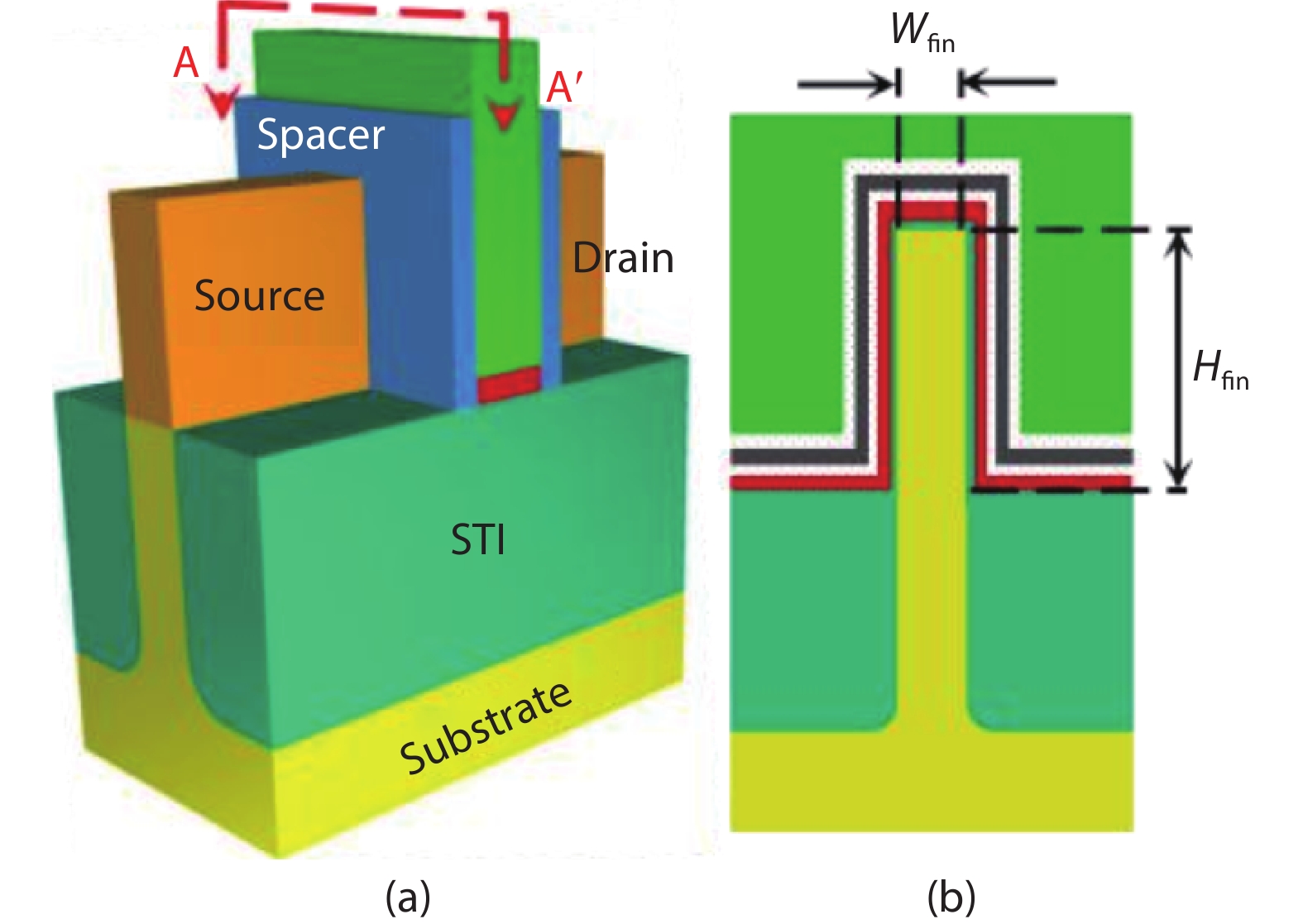
The devices used in this test are bulk nFinFETs produced by the process of 22 nm. The gate length of devices is 60 nm. Fig. 1 shows the structure diagram of the device. The channel of the device is a parallel fin-like structure with various fin numbers, 2, 4, 8 and 16, the effective width of single fin 2Hfin + Wfin = 80 nm, and the effective fin width of the device Weff = N(2Hfin + Wfin), where N is the fin number and working voltage VDD = 0.8 V. HfO2 and SiO2 are employed as the gate oxide. The devices are divided into two groups, while samples in group A are un-irradiated before hot-carrier stress and samples in group B are radiated before hot-carrier stress with different bias conditions during irradiation. There are some samples failed during the experiment because of ESD damage. The samples in group A were tested on a Keithley 4200 semiconductor parameter analyzer to conduct the hot carrier stress test. The stress condition used in this test was VGS = VDS = 1.2 V with the body and the source grounded. The total stress time was 6000 s. The IDS–VGS characteristics were obtained at the stress time of 1, 3.2, 10, 31.6, 100, 316.2, 1000, 3162.3, and 6000 s, respectively. When testing the IDS–VGS curve of the device, the drain voltage was set to 0.1 V, the body and source were grounded, and the gate voltage was increased from 0 to 0.8 V.
![]()
Figure 1.(Color online) The structure diagram of nFinFET. (a) A 3D model of bulk FinFET. (b) A cross-section view along A–A’ direction[
In addition, samples in group B were taken for the pre-irradiation test. The dose rate used for irradiation was 425.26 rad(Si)/s, and the total ionizing dose for 60 nm gate length samples was 2.5 Mrad(Si). There were three bias conditions: ON, OFF and TG, during irradiation for all the samples in group B. The ON bias condition was carried out with the gate applied with 0.8 V and other electrodes 0 V. The OFF bias condition was carried out with the drain applied with 0.8 V and other electrodes 0 V. The TG bias condition was carried out with the source and drain applied with 0.8 V and other electrodes 0 V. The floating annealing was carried on at room temperature for one week after irradiation. After annealing, the hot carrier stress test was carried out. The test conditions and process are the same as above.
3. Experimental results
Fig. 2 shows the degradation of VT for un-irradiated nFinFETs in group A with different fin numbers and gate length of 60nm under HCI stress. It is shown that as the stress time increases, the VT degradation percentage of 4 fin devices is significantly higher than the latter two with 8 fin and 16 fin.
![]()
Figure 2.(Color online) Degradation of
Fig. 3 shows the degradation of IDSAT for nFinFETs with different numbers of fins under HCI stress. We can see that there is also more degradation on devices with fewer fins. Fig. 4 shows IDS–VGS curves as a function of the irradiation dose for nFinFET with 8 fins and 60 nm gate length biased at ON state. As the dose increases, the IDS–VGS curve shifts positively, and VT and IDSAT increase.
![]()
Figure 3.(Color online) Degradation of saturation current (
![]()
Figure 4.
Fig. 5 shows the degradation of VT as a function of stress time for un-irradiated nFinFETs and irradiated nFinFETs in different bias conditions during irradiation. Table 1 shows the threshold voltage degradation percentage of un-irradiated and irradiated samples. The figure and the table indicate that the VT degradation of all devices under the hot carrier test decreases a lot, and the HCI of the irradiated devices weakens.
![]()
Figure 5.(Color online) Degradation of
Fig. 6 shows the degradation of IDSAT as a function of stress time for un-irradiated nFinFETs and irradiated nFinFETs in different bias conditions during irradiation. Table 2 shows the IDSAT degradation percentage of un-irradiated and irradiated samples. The figure and the table indicate that the channel IDSAT degradation of the four devices in the hot carrier test decreases successively, and the HCI of the irradiated devices weakens.
![]()
Figure 6.(Color online) Degradation of
4. Discussion and analysis
In a FinFET, all fins share one gate. As the gate voltage is positive, negative inversion charges are generated in the fins. Because the same charges repel each other, inversion charge density decreases in the adjacent fins. When the number of fins increases, the coupling effect between fins is more significant[
The Si–H bond exists at the interface between the gate oxide layer and silicon of FinFET[
For another reason, under the action of hot carrier stress, the hot electrons generated by the impact ionization at the drain end will be injected into the gate oxide layer and form oxide trap charges, which is why the VT drifts positively as the stress time increases[
![]()
Figure 7.(Color online) A schematic diagram showing that total dose irradiation causes trap holes in STI[
5. Conclusion
For bulk nFinFET produced by the 22 nm process, as the fin number increases, the charge density of the inversion layer inside the fin decreases due to the charge coupling between fins. In the hot carrier test, the more the fin number, the more the impact ionization weakened, the VT and channel IDSAT degradation are reduced, and thus the HCI is weakened. In the total dose irradiated device, the radiation has broken some Si-H bonds. In the subsequent HCI test, compared with the un-irradiated devices, the number of Si–H bonds affected by hot carriers decreases, and the degradation of device performance decreases. Moreover, the trapped charges generated by the radiation in the STI reduce the channel electric field. Therefore, HCI is weakened by total dose irradiation in nFinFET. Further investigation needs to be carried out for deeply mechanism analysis.
Acknowledgements
This work was supported by Youth Innovation Promotion Association CAS (2018473), the National Natural Science Foundation of China under Grant NO. 12075313, and the West Light Foundation of The Chinese Academy of Sciences (Grant No.2019-XBQNXZ-A-003).
References
[1] E X Zhang, D M Fleetwood, J A Hachtel et al. Total ionizing dose effects on strained Ge pMOS FinFETs on bulk Si. IEEE Trans Nucl Sci, 64, 226(2017).
[2] I Chatterjee, E X Zhang, B L Bhuva et al. Bias dependence of total-dose effects in bulk FinFETs. IEEE Trans Nucl Sci, 60, 4476(2013).
[3]
[4] W T Chang, L G Cin, W K Yeh. Impact of fin width and back bias under hot carrier injection on double-gate FinFETs. IEEE Trans Device Mater Reliab, 15, 86(2015).
[5]
[6]
[7]
[8] X Y Tang, J W Lu, R Zhang et al. Positive bias temperature instability and hot carrier injection of back gate ultra-thin-body In0.53Ga0.47As-on-insulator n-channel metal–oxide–semiconductor field-effect transistor. Chin Phys Lett, 32, 117302(2015).
[9] M Silvestri, S Gerardin, A Paccagnella et al. Channel hot carrier stress on irradiated 130-nm NMOSFETs: Impact of bias conditions during X-ray exposure. 2007 9th European Conference on Radiation and Its Effects on Components and Systems, 1(2007).
[10] Q W Zheng, J W Cui, H Zhou et al. Hot-carrier effects on total dose irradiated 65 nm n-type metal–oxide–semiconductor field-effect transistors. Chin Phys Lett, 33, 076102(2016).
[11]
[12] N C Das, V Nathan, S Dacus et al. Combined effects of hot-carrier stressing and ionizing radiation in SiO2, NO, and ONO MOSFETs. IEEE Electron Device Lett, 14, 40(1993).
[13] L Yang, Q Z Zhang, Y B Huang et al. Total ionizing dose response and annealing behavior of bulk nFinFETs with ON-state bias irradiaiton. IEEE Trans Nucl Sci, 65, 1503(2018).
[14]
[15] H Zhang, H Jiang, X Fan et al. Effects of total-ionizing-dose irradiation on single-event response for flip-flop designs at 14-/16-nm bulk FinFET technology node. IEEE Trans Nucl Sci, 65, 1928(2018).
[16] M P King, X Wu, M Eller et al. Analysis of TID process, geometry, and bias condition dependence in 14-nm FinFETs and implications for RF and SRAM performance. IEEE Trans Nucl Sci, 64, 285(2017).

Set citation alerts for the article
Please enter your email address
© Copyright 2018-2021 | Chinese Laser Press. All Rights Reserved 沪ICP备15018463号-20