
Chuen-Keung Sin, Jingzhao Zhang, Kinfai Tse, Junyi Zhu. A brief review of formation energies calculation of surfaces and edges in semiconductors[J]. Journal of Semiconductors, 2020, 41(6): 061101
- Journal of Semiconductors
- Vol. 41, Issue 6, 061101 (2020)
Abstract
1. Introduction
The fundamental thermodynamic theory of surfaces, initialized by the American scientist Josiah Willard Gibbs, is one of the most practical tools for the study of surface-related phenomena[
For surfaces of solids, especially metals and semiconductors, the surface energy is important in many related fields, determining the equilibrium shape of monocrystals, brittle fracture, or the rate of sintering. Wulff construction[
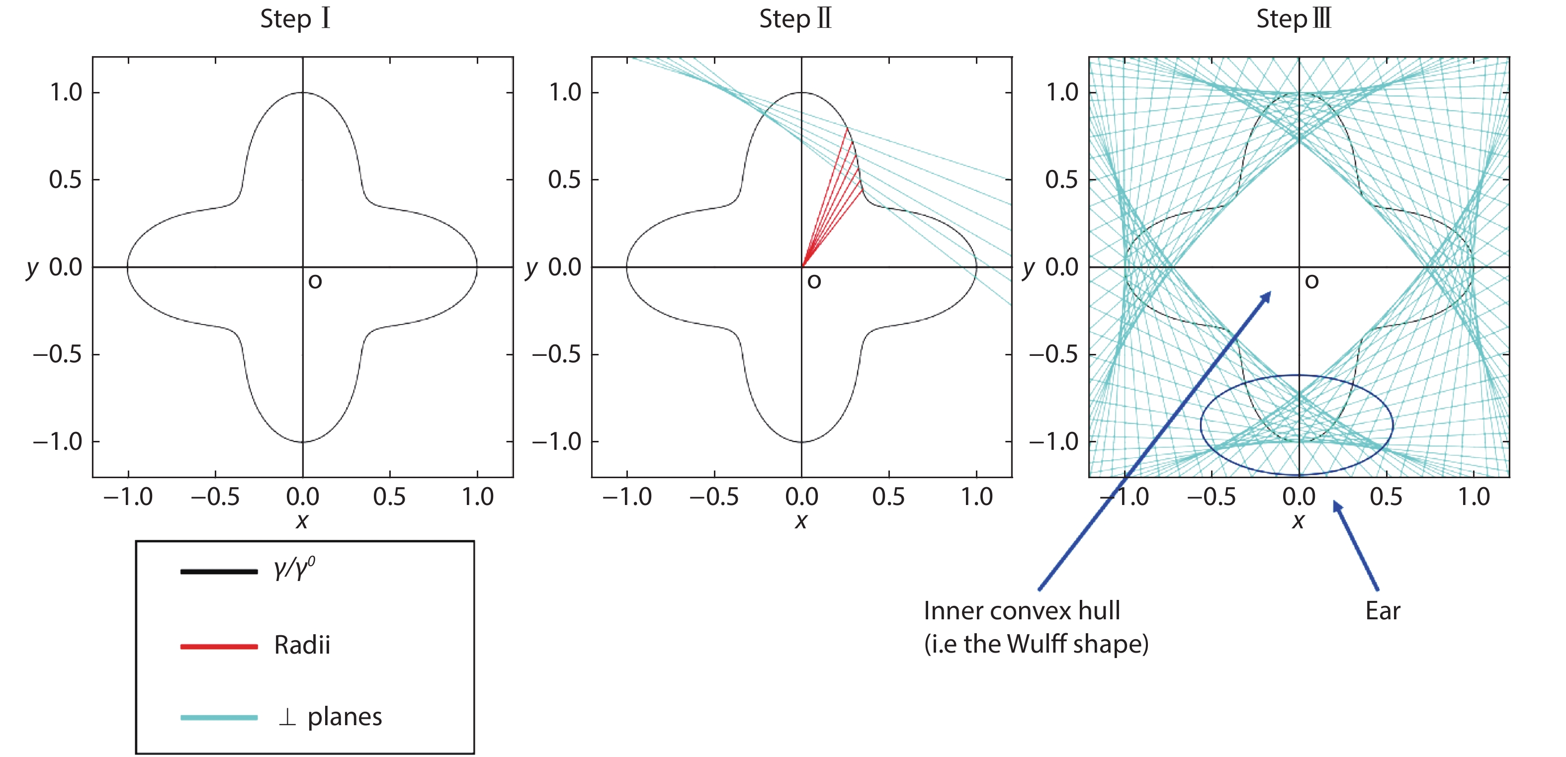
The anisotropy of surface free energy
![]()
Figure 1.(Color online) Workflow of Wulff construction: (I) draw a
where
Historically, among solids the surface energy of elemental crystals, mostly metals, was the earliest to be studied by researchers[
In the framework of DFT[
Before any algorithm is discussed, let us briefly have an overview on the history of the algorithm developments so as to have a general understanding of key advancements in the algorithm design of semiconductor surfaces and edges.
For non-polar surfaces, Feibelman, in 1983, used metallic Al and Mg crystal as examples to demonstrate the calculation of non-polar surface energies[
For polar surfaces, Chetty and Martin, in 1991, made the first attempt to calculate the absolute surface energy as an integral of local energy density[
For semi-polar surfaces, Li et al., in 2015, proposed a wedge scheme to find the energy difference between surfaces and a reference polar surface in the system of GaN[
For polar edges of 2D materials, Mukherjee et al., in 2011, presented a strategy with pure bare triangular clusters of h-BN in single size, each of which has only one type of exposed edge, to calculate the edge energies individually[
After the historical review, the algorithm designs for the calculation of different surface and edge energies are going to be discussed separately as follows.
Before diving into polar and semi-polar surfaces and polar edges, it is good to have a brief review on the non-polar surface or edges, and compare them with polar and semi-polar ones. For slab (ribbon) exposing non-polar surfaces (edges), the constituent elements are in the stoichiometric ratio within the whole structure. Therefore, there is no need to consider the chemical potential contribution from individual elements. Also, since the top and bottom surfaces are identical, it is possible to obtain the formation by assuming both surfaces have the same contribution to the total formation energy. This idea was first proposed by Feibelman in metallic materials[
where
where
where
For symmetric surface (edge for 2D lattice) pairs, the surface (edge) energy
where
![]()
Figure 2.(Color online) A slab created by cleaving a zinc-blende structure in (111) plane, grey and yellow atoms represent atom species A and B. Note the resultant upper and lower surface is of different termination.
2. Polar surfaces
At the earliest stage of polar surface study of semiconductors, fractionally charged pseudo hydrogen (pseudo-H) has been suggested to passivate one of the surfaces of the slab model so as to remove the charge transfer between surfaces[
Zhang and Wei[
![]()
Figure 3.(Color online) Wedge structure of size
A heterojunction supercell (Fig. 4) was also used to approximate unknown surface energies from known ones[
![]()
Figure 4.An illustration of a slab containing an interface and two passivated surfaces.
In Eq. (7), chemical potential has to be obtained from strained bulk simulation using the slab lattice constant to account for stress due to lattice mismatch. The heterojunction scheme is employed to study the (001) and (00
![]()
Figure 5.(Color online) A ZB(111)/WZ(001) heterojunction supercell consists of 6 WZ and ZB layers used in the calculation scheme of Tang
With the key assumption of localized energy contributions, the energy of an isolated crystal can be computed[
The passivated surface energy can then be systematically obtained by cancellation of bulk, edge and corner contributions. The transferability of such an estimation scheme mainly depends on 1) the ability of the proposed structure to capture the local bonding environment of the surface to be estimated, and 2) good size convergence of the proposed structure so that systematic cancellation of other contributions is possible. Zhang et al. proposed a tetrahedral cluster reproducing the same symmetry as the zinc-blende[
This estimation was shown to yield an acceptably accurate surface energy estimation[
![]()
Figure 6.(Color online) Tetrahedral cluster of zinc-blende structure of size
Calculation of 4 clusters of different sizes allows solutions for all unknowns (
With a fractional hydrogen[
Absolute interface energy is of equivalent physical interest including the determination of the wetting condition[
3. Semi-polar surfaces
Over the past few decades, even though the technologies in industrial application, like the quantum dot light-emitting diodes (LEDs)[
The definition of a semi-polar surface, with an example shown in Fig. 7, was initially made by Baker et al.[
![]()
Figure 7.(Color online) GaN crystal with 3 different types of surface cut. The semi-polar one is highlighted pink.
A comprehensive understanding of the absolute surface energies of all possible GaN surfaces is crucial to the estimation of equilibrium shape in the thermodynamic stability study, leading to important factors that can be used to modulate the crystallographic growth of GaN, which are regarded as the key issue in the realization of broadband and multi-color emission[
There is an early method proposed by Jindal and Shahedipour-Sandvik in 2009[
A 2D scheme of Wulff construction is applied to one of the cross-sections of GaN as indicated in Fig. 8. The length of
![]()
Figure 8.(Color online) Wulff construction of one of the 2D cross-sections of GaN. The yellow shaded area is a quarter of ECS in the cross-section. This strategy is from Ref. [
For this example,
![]()
Figure 9.(Color online) Workflow of finding the difference in crystal plane radii. Blue and black notations correspond to unrelaxed and relaxed surface structures respectively. This strategy is from Ref. [
However, based on the experimental observation from[
The acquisition of accurate energies of semi-polar surfaces is particularly difficult for three reasons: firstly, the conventional slab method cannot be used to deal with individual semi-polar surfaces resulting from the structural asymmetry; secondly, large computational input in the form of wedges, usually with high index planes, are involved which leads to high computational cost; thirdly, as semi-polar surfaces are sometimes of a step nature, it is not always feasible to passivate the bottom surfaces of slabs with pseudo-H atoms in the absence of significant unphysical charge transfer and steric effect, which deteriorates the result accuracy[
To overcome these mentioned difficulties, Zhang et al. introduced a fundamentally different algorithm in 2018, using GaN as an example[
![]()
Figure 10.(Color online) (a) and (b) are slabs with upper semi-polar surfaces of m- and a-family, respectively, and with bottom side cut into step-structure in which the non-polar and polar surfaces are passivated by either H or pseudo-H. These figures are adapted from Ref. [
According to Eq. (3),
where
where
However, taking the semi-polar surface (11
![]()
Figure 11.(Color online) Slab with a well being cut with width and depth as
where
Zhang has used a slab with both sides cut with a zigzag structure to implement the convergence test to give a residual error less than 1.5 meV/Å2, indicating the high accuracy of the method. This new algorithm to estimate the absolute energy of semi-polar surface is completely different from the traditional methods which are based on wedges and slabs. It is because this new method is applicable to an arbitrary surface as long as we can passivate the polar and non-polar planes at the bottom surface with zigzag structure.
Later on another Japanese group, Seta et al., published some literature in 2019 using both slabs and wedges to estimate the absolute energy of semi-polar surfaces[
![]()
Figure 12.(Color online) Cross section view of AlN triangular wedge with surface (
After calculating the energies of wedges in Fig. 12 for different sizes, the same procedures were repeated by interchanging the position of Al and N atoms. Therefore, the energy difference (here we use the notation
where
where
Seta has given one more improvement on the temperature dependence on the estimation of surface energies by including the translational, rotational and vibrational motion of atoms in gaseous phase into the chemical potential
where
Nearly at the same time, Akiyama, from the same Japanese group, proposed another algorithm to calculate the energy of polar and semi-polar surfaces simultaneously[
4. Polar edges of 2D materials
In the world of 2D materials, graphene is the system that was first discovered and the most intensively studied[
In recent years, the family of 2D materials has grown larger, including compounds such as hexagonal boron nitride (h-BN) that is an insulator, and molybdenum dichalcogenides (
To understand various equilibrium shapes in experiments, obtaining the energies of different edges are crucial. Due to the structural asymmetry of the nanoribbon of these compounds, as shown in Fig. 13, edges with polarities emerge. The direct calculation of polar edge energy is no longer achievable because the early method used in graphene can only estimate the average energies of two opposite zigzag edges in the ribbons[
![]()
Figure 13.(Color online) (a)/(c) and (b)/(d) are the (top view/side view) of h-BN and
In the past few years, several groups have developed their own methods to estimate the absolute energy of polar edges. Most of them are based on the creation of triangular nanoclusters terminated at the edges with the same polarity[
In all methods, polar edge energies can be obtained under different chemical potentials. The range of the chemical potentials can be obtained from a standard calculation of phase diagram of various secondary phases of the compound, which has been widely applied in the energy calculations of point defects, surfaces, and interfaces[
Besides chemical potential, passivation of edges is the key to the calculation of edge energy. For early methods, passivation was not taken into the consideration[
The first theoretical attempt was made by estimating the average energies of h-BN edges terminated by B and N[
where
![]()
Figure 14.(Color online) (a) The computational setup for triangular clusters with green dots as boron atoms and silver dots as nitrogen atoms. (b) The result of equilibrium shapes at different chemical potential ranges[
The results suggest that it is possible for armchair-edged hexagon to exist at the mid-range of chemical potential. In addition, other literature gives the same computational prediction on the stability of the armchair edge[
The bare triangular cluster was reported to contain corner distortions and inter-edge couplings[
Another method proposed by Cao et al. to find the equilibrium shape of MoS2[
![]()
Figure 15.(Color online) (a) The
where
where
![]()
Figure 16.(Color online) Equilibrium shape of
From the Wulff construction, the S-terminated triangular shape can be observed in an S-rich condition in which the shape matches the experimental results[
Before entering the last example, it is good to mention that the method of Cao's example is suitable for obtaining a fast calculation. Yet, there is another method proposed by Zhang et al.[
![]()
Figure 17.(Color online) B, N and H atoms are denoted by pink, blue and white spheres respectively. (a) Passivated and unpassivated zigzag and armchair edges. (b) Reconstruction of seven- and five- rings on the ZZN and ZZB edges, respectively. (c) Ribbon of bottom zigzag edged passivated with hydrogen and arbitrary configuration on the upper zigzag edge. (d) N-terminated passivated triangular cluster of size
where
Therefore, instead of a direct calculation of edge energy from the bare triangular cluster, the chemical potentials of passivating hydrogens have to be first estimated from the passivated cluster. The reason for the more reliable calculation of the chemical potential of passivating hydrogen than the edge energy of the bare triangle is that the passivation helps to reduce corner distortion and the unphysical charge transfer[
where m is the cluster size and
where
There are three red-colored parameters to be fitted
![]()
Figure 18.(Color online) Total energy of H-passivated triangular clusters with different size (
After the estimation of hydrogen chemical potential, the half-passivated ribbon with arbitrary configuration on the upper edge (Fig. 17(c)) can be calculated to obtain the absolute energy of the particular polar edge by Eq. (22). Also, Zhang has proposed a self-consistency check to ensure the accuracy of the algorithm by calculating the residual error Er. Er can be calculated by Eq. (26) after the calculation of total energy of both sides passivated ribbon Ep. Zhang has shown the error is reduced from 3.43% to 0.12% when compared with the bare triangular method.
After that, Zhang had shown in Fig. 3 of their literature[
where
to obtain
![]()
Figure 19.(Color online) Equilibrium shapes of h-BN nanocluster under different chemical potentials at 1300 K, consisting of H-passivated edges. Yellow, green and black lines are of ZZBH, ZZNH and ARMH edges respectively. The figure is adapted from Ref. [
After the discussion of several methods of calculating the polar edge energy, the last one proposed by Zhang, is able to capture more physical pictures and also gives the highest accuracy because it includes the temperature effect and passivation which leads to stabilization effect to all type of edges. It is also capable of revealing the important role played by hydrogen atoms in the growth of 2D h-BN monolayer.
5. Conclusion
We have reviewed some important historical algorithms on the assessment of surface and edge stability of various semiconducting compounds. The key concept for a successful algorithm is to eliminate the long range charge transfer and interaction of different surfaces or edges by passivating dangling bonds and mimicking the electronic environment of the desired surfaces or edges. In addition, not all passivation can yield a reliable result because an electron counting model has to be satisfied and steric effects should be avoided. To estimate the localized steric effects, it is possible to perform further simulation that can mimic the stressed local configuration. Still, further investigations of quasi-2D structures are highly important, yet largely missing because they lack effective passivation schemes on the edges. With all the technological advancements, we can safely conclude that a highly accurate algorithm combining a reasonable analysis of passivation and temperature effects can have strong predictive power in the equilibrium shape under various growth conditions and the dawn of a highly effective collaboration between theoreticians and experimentalists may largely improve the field of crystal growth and device fabrication of semiconductors.
Acknowledgements
The research is supported by HKRGC, GRF with the Project Codes of 14307219, 14307018, 14301318, and 14319416; and by direct grant from CUHK. .
References
[1] N C Bristowe, P B Littlewood, E Artacho. Surface defects and conduction in polar oxide heterostructures. J Phys B, 83, 205405(2011).
[2] S Kahwaji, R A Gordon, E D Crozier et al. Surfactant-mediated growth of ferromagnetic Mn-doped Si. Phys Rev B, 88, 174419(2013).
[3] J Zhang, W Zhao, J Zhu. Missing links towards understanding the equilibrium shapes of hexagonal boron nitride: algorithm, hydrogen passivation, and temperature effects. Nanoscale, 10, 17683(2018).
[4] C Tang, M J S Spencer, A S Barnard. Activity of ZnO polar surfaces: an insight from surface energies. Phys Chem Chem Phys, 16, 22139(2014).
[5] R Dingreville, J Qu, M Cherkaoui. Surface free energy and its effect on the elastic behavior of nano-sized particles, wires and films. J Mech Phys Solids, 53, 1827(2005).
[6]
[7] G Wulff. Xxv. zur frage der geschwindigkeit des wachsthums und der auflösung der krystallflächen. Zeitschrift für Kristallographie - Crystalline Materials, 34, 449(1901).
[8] M P Curie. Sur la formation des cristaux et sur les constantes capillaires de leurs différentes faces. Bull Soc Fr Mineral, 8, 145(1885).
[9] H Li, L Geelhaar, H Riechert et al. Computing equilibrium shapes of wurtzite crystals: The example of GaN. Phys Rev Lett, 115, 085503(2015).
[10] N D Lang, W Kohn. Theory of metal surfaces: Charge density and surface energy. Phys Rev B, 1, 4555(1970).
[11] R J Jaccodine. Surface energy of germanium and silicon. J Electrochem Soc, 110, 524(1963).
[12] W R Tyson, W A Miller. Surface free energies of solid metals: Estimation from liquid surface tension measurements. Surf Sci, 62, 267(1977).
[13] Boer F R de, R Boom, W C M Mattens et al. Cohesion in metals: Transition metal alloys. Elsevier Scientific Pub. Co.(1988).
[14] H P Bonzel, A Emundts. Absolute values of surface and step free energies from equilibrium crystal shapes. Phys Rev Lett, 84, 5804(2000).
[15] H P Bonzel, M Nowicki. Absolute surface free energies of perfect low-index orientations of metals and semiconductors. Phys Rev B, 70, 245430(2004).
[16] A K Niessen, A R Miedema, Boer F R de et al. Enthalpies of formation of liquid and solid binary alloys based on 3d metals: IV. alloys of cobalt. Physica B+C, 151, 401(1988).
[17] K C Mills, Y C Su. Review of surface tension data for metallic elements and alloys: Part 1-pure metals. Int Mater Rev, 51, 329(2006).
[18] B J Keene. Review of data for the surface tension of pure metals. Int Mater Rev, 38, 157(1993).
[19] J Y Lee, M Punkkinen, S Schönecker et al. The surface energy and stress of metals. Surf Sci, 674, 51(2018).
[20] J P Perdew, H Q Tran, E D Smith. Stabilized jellium: Structureless pseudopotential model for the cohesive and surface properties of metals. Phys Rev B, 42, 11627(1990).
[21] H L Skriver, N M Rosengaard. Surface energy and work function of elemental metals. Phys Rev B, 46, 7157(1992).
[22] H Erschbaumer, A J Freeman, C L Fu et al. Surface states, electronic structure and surface energy of the Ag (001) surface. Surf Sci, 243, 317(1991).
[23] R J Needs, M Mansfield. Calculations of the surface stress tensor and surface energy of the (111) surfaces of iridium, platinum and gold. J Phys Condens Matter, 1, 41(1989).
[24] L Vitos, A Ruban, H Skriver et al. The surface energy of metals. Surf Sci, 411, 186(1998).
[25] I Galanakis, N Papanikolaou, P H Dederichs. Applicability of the broken-bond rule to the surface energy of the fcc metals. Surf Sci, 511, 1(2002).
[26] M Methfessel, D Hennig, M Scheffler. Trends of the surface relaxations, surface energies, and work functions of the 4d transition metals. Phys Rev B, 46, 4816(1992).
[27] A M Rodríguez, G Bozzolo, J Ferrante. Multilayer relaxation and surface energies of fcc and bcc metals using equivalent crystal theory. Surf Sci, 289, 100(1993).
[28] R Tran, Z Xu, B Radhakrishnan et al. Surface energies of elemental crystals. Sci Data, 3, 160080(2016).
[29] P Hohenberg, W Kohn. Inhomogeneous electron gas. Phys Rev, 136, B864(1964).
[30] W Kohn, L J Sham. Self-consistent equations including exchange and correlation effects. Phys Rev, 140, A1133(1965).
[31] W A Harrison. Theory of polar semiconductor surfaces. J Vac Sci Technol, 16, 1492(1979).
[32] P W Tasker. The stability of ionic crystal surfaces. J Phys C, 12, 4977(1979).
[33] S Nakamura, T Mukai, M Senoh. Candel-class high-brightness InGaN/AlGaN double-heterostructure blue-light-emitting diodes. Appl Phys Lett, 64, 1687(1994).
[34] S Nakamura, M Senoh, S I Nagahama et al. InGaN-based multi-quantum-well-structure laser diodes. Jpn J Appl Phys, 35, L74(1996).
[35] S Nakamura. The roles of structural imperfections in InGaN-based blue light-emitting diodes and laser diodes. Science, 281, 956(1998).
[36] S Nakamura, S Pearton, G Fasol. The blue laser diode: The complete story. Springer(2000).
[37] D M Bagnall, Y F Chen, Z Zhu et al. Optically pumped lasing of zno at room temperature. Appl Phys Lett, 70, 2230(1997).
[38] Ü Özgür, Y I Alivov, C Liu et al. A comprehensive review of ZnO materials and devices. J Appl Phys, 99, 041301(2005).
[39] L Guo, Y L Ji, H B Xu et al. Regularly shaped, single-crystalline ZnO nanorods with wurtzite structure. J Am Chem Soc, 124, 14864(2002).
[40] B Liu, Y Bando, C Tang et al. Wurtzite-type faceted single-crystalline gan nanotubes. Appl Phys Lett, 88, 093120(2006).
[41] Y Zhang, J Zhu. Surfactant antimony enhanced indium incorporation on ingan (000-1) surface: A dft study. J Cryst Growth, 438, 43(2016).
[42] P J Feibelman. Static quantum-size effects in thin crystalline, simple-metal films. Phys Rev B, 27, 1991(1983).
[43] N Chetty, R M Martin. Determination of integrals at surfaces using the bulk crystal symmetry. Phys Rev B, 44, 5568(1991).
[44] S B Zhang, S H Wei. Surface energy and the common dangling bond rule for semiconductors. Phys Rev Lett, 92, 086102(2004).
[45] J Y Rempel, B L Trout, M G Bawendi et al. Properties of the CdSe (0001), (000-1), and (11-20) single crystal surfaces: Relaxation, reconstruction, and adatom and admolecule adsorption. J Phys Chem B, 109, 19320(2005).
[46] A Jenichen, C Engler, B Rauschenbach. Comparison of wurtzite and zinc-blende GaAs surfaces as possible nanowire side walls: Dft stability calculations. Surf Sci, 613, 74(2013).
[47] Y Zhang, J Zhang, K Tse et al. Pseudo-hydrogen passivation: A novel way to calculate absolute surface energy of zinc blende (111)/(-1-1-1) surface. Sci Rep, 6, 20055(2016).
[48] Y Zhang, J Zhang, J Zhu. Stability of wurtzite semipolar surfaces: Algorithms and practices. Phys Rev Mater, 2, 073401(2018).
[49] Y Seta, T Akiyama, A M Pradipto et al. Absolute surface energies of semipolar planes of aln during metalorganicvapor phase epitaxy growth. J Cryst Growth, 510, 7(2019).
[50] R Mukherjee, S Bhowmick. Edge stabilities of hexagonal boron nitride nanoribbons: A first-principles study. J Chem Theory Comput, 7, 720(2011).
[51] D Cao, T Shen, P Liang et al. Role of chemical potential in flake shape and edge properties of monolayer MoS2. J Phys Chem C, 119, 4294(2015).
[52] K Rapcewicz, B Chen, B Yakobson et al. Consistent methodology for calculating surface and interface energies. Phys Rev B, 57, 7281(1998).
[53] K Shiraishi. A new slab model approach for electronic structure calculation of polar semiconductor surface. J Phys Soc Jpn, 59, 3455(1990).
[54] N Chetty, R M Martin. First-principles energy density and its applications to selected polar surfaces. Phys Rev B, 45, 6074(1992).
[55] J A Appelbaum, G A Baraff, D R Hamann. GaAs(100): Its spectrum, effective charge, and reconstruction patterns. Phys Rev B, 14, 1623(1976).
[56] N Chetty, R M Martin. GaAs (111) and (1’-.2m”.3m’ ’.2m”-.3m’ 1’-.2m”.3m’ ’.2m”-.3m’ 1’-.2m”.3m’ ’.2m”-.3m’) surfaces and the GaAs/AlAs (111) heterojunction studied using a local energy density. Phys Rev B, 45, 6089(1992).
[57] N Moll, A Kley, E Pehlke et al. GaAs equilibrium crystal shape from first principles. Phys Rev B, 54, 8844(1996).
[58] L Manna, R Wang et al. First-principles modeling of unpassivated and surfactant-passivated bulk facets of wurtzite CdSe: A model system for studying the anisotropic growth of CdSe nanocrystals. J Phys Chem B, 109, 6183(2005).
[59] C E Dreyer, A Janotti, C G Van de Walle. Absolute surface energies of polar and nonpolar planes of GaN. Phys Rev B, 89, 081305(2014).
[60] J Zhang, Y Zhang, K Tse et al. New approaches for calculating absolute surface energies of wurtzite (0001)/(000-1): A study of ZnO and GaN. J Appl Phys, 119, 205302(2016).
[61] J Zhang, Y Zhang, K Tse et al. Hydrogen-surfactant-assisted coherent growth of GaN on ZnO substrate. Phys Rev Mater, 2, 013403(2018).
[62] T Akiyama, H Nakane, K Nakamura et al. Effective approach for accurately calculating individual energy of polar heterojunction interfaces. Phys Rev B, 94, 115302(2016).
[63] J V Pezold, P D Bristowe. Atomic structure and electronic properties of the GaN/ZnO (0001) interface. J Mater Sci, 40, 3051(2005).
[64] A B Yankovich, B Puchala, F Wang et al. Stable p-type conduction from Sb-decorated head-to-head basal plane inversion domain boundaries in ZnO nanowires. Nano Lett, 12, 1311(2012).
[65] M Wong, K Tse, J Zhu. New types of CZTS3112 grain boundaries: Algorithms to passivation. J Phys Chem C, 122, 7759(2018).
[66] X Dai, Y Deng, X Peng et al. Quantum-dot light-emitting diodes for large-area displays: Towards the dawn of commercialization. Adv Mater, 29, 1607022(2017).
[67] E Jang, S Jun, H Jang et al. White-light-emitting diodes with quantum dot color converters for display backlights. Adv Mater, 22, 3076(2010).
[68] H Masui, S Nakamura, S P DenBaars et al. Nonpolar and semipolar III-nitride light-emitting diodes: Achievements and challenges. IEEE Trans Electron Devices, 57, 88(2010).
[69] I Ho, G B Stringfellow. Solid phase immiscibility in GaInN. Appl Phys Lett, 69, 2701(1996).
[70] T Matsuoka. Unstable mixing region in wurtzite In1–
[71] A Koukitu, Y Kumagai. Thermodynamic analysis of group III nitrides grown by metal-organic vapour-phase epitaxy (MOVPE), hydride (or halide) vapour-phase epitaxy (HVPE) and molecular beam epitaxy (MBE). J Phys Condens Matter, 13, 32(2001).
[72] M Funato, M Ueda, Y Kawakami et al. Blue, green, and amber InGaN/GaN light-emitting diodes on semipolar {11-22} GaN bulk substrates. Jpn J Appl Phys, 45, 24(2006).
[73] T Wunderer, P Brückner, B Neubert et al. Bright semipolar GaInN/GaN blue light emitting diode on side facets of selectively grown GaN stripes. Appl Phys Lett, 89, 041121(2006).
[74] H Sato, R B Chung, H Hirasawa et al. Optical properties of yellow light-emitting diodes grown on semipolar (11-22) bulk GaN substrates. Appl Phys Lett, 92, 221110(2008).
[75] J E Northrup. GaN and InGaN (11-22) surfaces: Group-III adlayers and indium incorporation. Appl Phys Lett, 95, 133107(2009).
[76] Y Zhao, Q Yan, C Y Huang et al. Indium incorporation and emission properties of nonpolar and semipolar InGaN quantum wells. Appl Phys Lett, 100, 201108(2012).
[77] M Monavarian, S Metzner, N Izyumskaya et al. Indium-incorporation efficiency in semipolar (11-22) oriented InGaN-based light emitting diodes. SPIE OPTO, 9363, 2P(2015).
[78] R Bhat, G M Guryanov. Experimental study of the orientation dependence of indium incorporation in GaInN. J Cryst Growth, 433, 7(2016).
[79] T Wang. Topical review: Development of overgrown semi-polar GaN for high efficiency green/yellow emission. Semicond Sci Technol, 31, 093003(2016).
[80] T Takeuchi, H Amano, I Akasaki. Theoretical study of orientation dependence of piezoelectric effects in wurtzite strained GaInN/GaN heterostructures and quantum wells. Jpn J Appl Phys, 39, 413(2000).
[81] D A B Miller, D S Chemla, T C Damen et al. Band-edge electroabsorption in quantum well structures: The quantum-confined stark effect. Phys Rev Lett, 53, 2173(1984).
[82] T Takeuchi, S Sota, M Katsuragawa et al. Quantum-confined stark effect due to piezoelectric fields in GaInN strained quantum wells. Jpn J Appl Phys, 36, L382(1997).
[83] T J Baker, B A Haskell, F Wu et al. Characterization of planar semipolar gallium nitride films on spinel substrates. Jpn J Appl Phys, 44, L920(2005).
[84] C Herring. Some theorems on the free energies of crystal surfaces. Phys Rev, 82, 87(1951).
[85] D Du, D J Srolovitz, M E Coltrin et al. Systematic prediction of kinetically limited crystal growth morphologies. Phys Rev Lett, 95, 155503(2005).
[86] Y Enya, Y Yoshizumi, T Kyono et al. 531 nm green lasing of ingan based laser diodes on semi-polar 20-21 free-standing GaN substrates. Appl Phys Express, 2, 082101(2009).
[87] C Liu, A Šatka, L J Krishnan et al. Light emission from InGaN quantum wells grown on the facets of closely spaced GaN nano-pyramids formed by nano-imprinting. Appl Phys Express, 2, 121002(2009).
[88] W Bergbauer, M Strassburg, C Kölper et al. Continuous-flux movpe growth of position-controlled N-face GaN nanorods and embedded ingan quantum wells. Nanotechnology, 21, 305201(2010).
[89] B Leung, Q Sun, C D Yerino et al. Using the kinetic wulff plot to design and control nonpolar and semipolar GaN heteroepitaxy. Semicond Sci Technol, 27, 024005(2012).
[90] Y H Ko, J Song, B Leung et al. Multi-color broadband visible light source via GaN hexagonal annular structure. Sci Rep, 4, 5514(2014).
[91] B Foltynski, N Garro, M Vallo et al. The controlled growth of GaN microrods on Si (111) substrates by MOCVD. J Cryst Growth, 414, 200(2015).
[92] V Jindal, F Shahedipour-Sandvik. Theoretical prediction of GaN nanostructure equilibrium and nonequilibrium shapes. J Appl Phys, 106, 083115(2009).
[93] M Mandl, X Wang, T Schimpke et al. Group III nitride core-shell nano- and microrods for optoelectronic applications. Phys Status Solidi RRL, 7, 800(2013).
[94] M D Pashley. Electron counting model and its application to island structures on molecular-beam epitaxy grown GaAs (001) and ZnSe (001). Phys Rev B, 40, 10481(1989).
[95] A Kusaba, Y Kangawa, P Kempisty et al. Thermodynamic analysis of (0001) and (000-1) GaN metalorganic vapor phase epitaxy. Jpn J Appl Phys, 56, 070304(2017).
[96] T Akiyama, Y Seta, K Nakamura et al. Modified approach for calculating individual energies of polar and semipolar surfaces of group-III nitrides. Phys Rev Mater, 3, 023401(2019).
[97] X Zhang, J Xin, F Ding. The edges of graphene. Nanoscale, 5, 2556(2019).
[98] V I Artyukhov, Y Liu, B I Yakobson. Equilibrium at the edge and atomistic mechanisms of graphene growth. Proc Natl Acad Sci USA, 109, 15136(2012).
[99] C K Gan, D J Srolovitz. First-principles study of graphene edge properties and flake shapes. Phys Rev B, 81, 125445(2010).
[100] V I Artyukhov, Y Hao, R S Ruoff et al. Breaking of symmetry in graphene growth on metal substrates. Phys Rev Lett, 114, 115502(2015).
[101] S Okada. Energetics of nanoscale graphene ribbons: Edge geometries and electronic structures. Phys Rev B, 77, 041408(2008).
[102] K S Novoselov, A Mishchenko, A Carvalho et al. 2D materials and van der waals heterostructures. Science, 353, aac9439(2016).
[103] Y Stehle, H M Meyer, R R Unocic et al. Synthesis of hexagonal boron nitride monolayer: Control of nucleation and crystal morphology. Chem Mater, 27, 8041(2015).
[104] S Y Yang, G W Shim, S B Seo et al. Effective shape-controlled growth of monolayer MoS2 flakes by powderbased chemical vapor deposition. Nano Res, 10, 255(2017).
[105] Y Chen, P Cui, X Ren et al. Fabrication of MoSe2 nanoribbons via an unusual morphological phase transition. Nat Commun, 8, 15135(2017).
[106] J Li, Z Hu, Y Yi et al. Hexagonal boron nitride growth on Cu–Si alloy: Morphologies and large domains. Small, 15, 1805188(2019).
[107] Y Liu, S Bhowmick, B I Yakobson. Bn white graphene with ”colorful” edges: The energies and morphology. Nano Lett, 11, 3113(2011).
[108] E Machlin. Aspects of thermodynamics and kinetics relevant to materials science. Elsevier Science(2007).
[109] K Tse, M Wong, Y Zhang et al. Defect properties of Na and K in Cu2ZnSnS4 from hybrid functional calculation. J Appl Phys, 124, 165701(2018).
[110] J Gao, J Yip, J Zhao et al. Graphene nucleation on transition metal surface: Structure transformation and role of the metal step edge. J Am Chem Soc, 133, 5009(2011).
[111] J Coraux, A T N’Diaye, M Engler et al. Growth of graphene on Ir (111). New J Phys, 11, 039801(2009).
[112] X Song. Chemical vapor deposition growth of large-scale hexagonal boron nitride with controllable orientation. Nano Res, 8, 3164(2015).
[113] B Huang, H Lee, B L Gu et al. Edge stability of boron nitride nanoribbons and its application in designing hybrid bnc structures. Nano Res, 5, 62(2012).
[114] A Du, Y Chen, Z Zhu et al. Dots versus antidots: Computational exploration of structure, magnetism, and half metallicity in boron-nitride nanostructures. J Am Chem Soc, 131, 17354(2009).
[115] der Zande A M Van, P Y Huang, D A Chenet et al. Grains and grain boundaries in highly crystalline monolayer molybdenum disulphide. Nat Mater, 12, 554(2013).
[116] J V Lauritsena, M V Bollinger, E Lægsgaarda et al. Atomic-scale insight into structure and morphology changes of MoS2 nanoclusters in hydrotreating catalysts. J Catal, 221, 510(2004).
[117] I Barin. Thermochemical data of pure substances. Wiley-VCH Verlag GmbH(2008).

Set citation alerts for the article
Please enter your email address
© Copyright 2018-2021 | Chinese Laser Press. All Rights Reserved 沪ICP备15018463号-20