• Photonics Research
  • Vol. 5, Issue 2, A30 (2017)
Anna Kafar1、*, Szymon Stanczyk1, Marcin Sarzynski1, Szymon Grzanka1、2, Jakub Goss1, Irina Makarowa2, Anna Nowakowska-Siwinska2, Tadek Suski1, and Piotr Perlin1、2
Author Affiliations
  • 1Institute of High Pressure Physics, Polish Academy of Sciences, Sokolowska 29/37, 01-142 Warsaw, Poland
  • 2TopGaN Ltd., Sokolowska 29/37, 01-142 Warsaw, Poland
  • show less
    DOI: 10.1364/PRJ.5.000A30 Cite this Article Set citation alerts
    Anna Kafar, Szymon Stanczyk, Marcin Sarzynski, Szymon Grzanka, Jakub Goss, Irina Makarowa, Anna Nowakowska-Siwinska, Tadek Suski, Piotr Perlin. InAlGaN superluminescent diodes fabricated on patterned substrates: an alternative semiconductor broadband emitter[J]. Photonics Research, 2017, 5(2): A30 Copy Citation Text show less
    Schemes of popular SLD waveguide geometries: (a) tilted facet, (b) tilted waveguide, (c) waveguide with an absorber section, and (d) bent waveguide (used in this study).
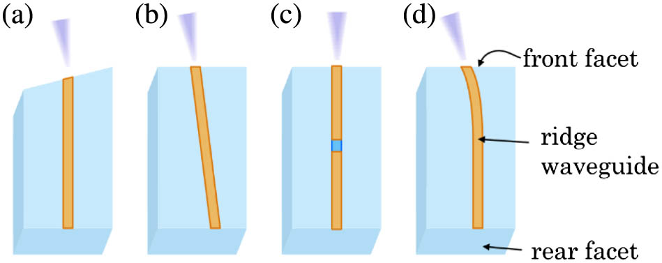
    Fig. 1. Schemes of popular SLD waveguide geometries: (a) tilted facet, (b) tilted waveguide, (c) waveguide with an absorber section, and (d) bent waveguide (used in this study).
    Simulated changes in emission spectra shape resulting from light amplification in medium with a linear profile of indium.
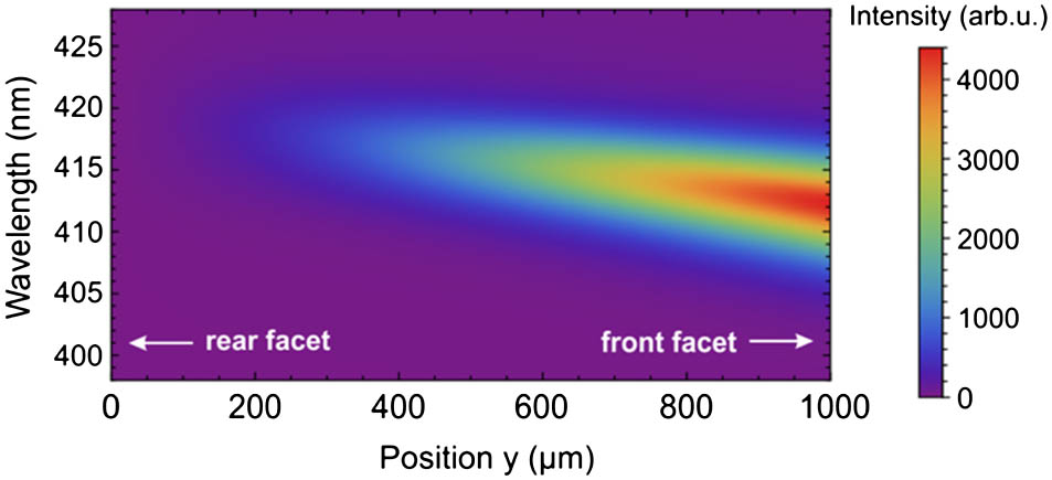
    Fig. 2. Simulated changes in emission spectra shape resulting from light amplification in medium with a linear profile of indium.
    Example of a calculated emission spectrum of an SLD with a step-like indium content profile along the waveguide.
    Fig. 3. Example of a calculated emission spectrum of an SLD with a step-like indium content profile along the waveguide.
    Fabricated step vicinal angle profile. The inset presents a 3D scheme of the surface pattern.
    Fig. 4. Fabricated step vicinal angle profile. The inset presents a 3D scheme of the surface pattern.
    Scheme of the epitaxial structure design of the examined samples (indium content estimated for a non-patterned wafer).
    Fig. 5. Scheme of the epitaxial structure design of the examined samples (indium content estimated for a non-patterned wafer).
    Microphotoluminescence maps of central emission wavelength measured for substrate areas with three types of patterns: (a) flat, (b) linear, and (c) step.
    Fig. 6. Microphotoluminescence maps of central emission wavelength measured for substrate areas with three types of patterns: (a) flat, (b) linear, and (c) step.
    Optical power versus current curves measured for all types of devices.
    Fig. 7. Optical power versus current curves measured for all types of devices.
    Comparison of emission spectra measured for three types of SLDs: fabricated on a substrate with constant vicinal angle (flat), with a linear profile of vicinal angle (linear), and with a step-like profile (step). The measurement was performed under 250 mA of operating current.
    Fig. 8. Comparison of emission spectra measured for three types of SLDs: fabricated on a substrate with constant vicinal angle (flat), with a linear profile of vicinal angle (linear), and with a step-like profile (step). The measurement was performed under 250 mA of operating current.
    Evolution of the emission spectrum with applied current measured for SLD fabricated on a substrate with step-like indium content profile.
    Fig. 9. Evolution of the emission spectrum with applied current measured for SLD fabricated on a substrate with step-like indium content profile.
    Anna Kafar, Szymon Stanczyk, Marcin Sarzynski, Szymon Grzanka, Jakub Goss, Irina Makarowa, Anna Nowakowska-Siwinska, Tadek Suski, Piotr Perlin. InAlGaN superluminescent diodes fabricated on patterned substrates: an alternative semiconductor broadband emitter[J]. Photonics Research, 2017, 5(2): A30
    Download Citation