Abstract
We demonstrate InGaN violet light-emitting superluminescent diodes with large spectral width suitable for applications in optical coherence spectroscopy. This was achieved using the concept of nonlinear indium content profile along the superluminescent diode waveguide. A specially designed 3D substrate surface shape leads to a step-like indium content profile, with the indium concentration in the InGaN/GaN quantum wells ranging approximately between 6% and 10%. Thanks to this approach, we were able to increase the width of the spectrum in processed devices from 2.6 nm (reference diode) to 15.5 nm.1. INTRODUCTION
For most popular light-emitting diode (LED) applications such as general lightning or signalization, the greatest concerns are optical power, robustness, and lifetime. However, there are also applications which require a light source characterized by broad emission spectra and, at the same time, easy coupling to an optical fiber. Most popular examples are fiber optic gyroscopes (FOG) and optical coherence tomography (OCT). In these cases, a popular solution is a superluminescent diode (SLD), an emitter fabricated in a very similar way to a laser diode but which cannot reach lasing threshold due to additional (usually mirror) losses (Fig. 1). In the field of infrared SLDs, a lot of effort has been devoted to broadening the emission spectra and by this means increase the capabilities of the mentioned applications. This includes, among others, fabricating an active region consisting of quantum wells (QWs) having different widths [1], containing quantum dots [2–4] or even dash-in-well structures [5], and often utilizing light emission based on two energy levels [4–6].
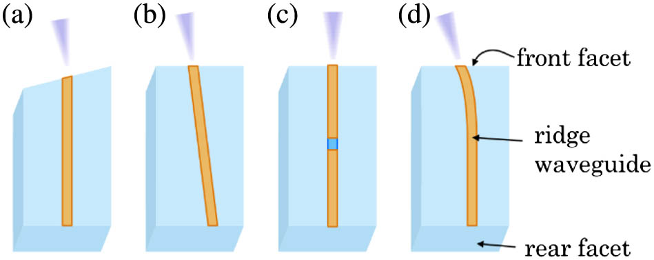
Figure 1.Schemes of popular SLD waveguide geometries: (a) tilted facet, (b) tilted waveguide, (c) waveguide with an absorber section, and (d) bent waveguide (used in this study).
The subject of nitride SLDs emerged in 2009 with the paper of Feltin et al. [7]. Since then, many groups have contributed their work into studying SLD properties and optimizing their work parameters [8–10]. Reaching high optical powers [11,12], even above 350 mW [13], can be regarded as a proof of the maturity of this research field. At this point, it is important to work toward meeting the requirements of possible applications. In contrast to infrared devices, nitride SLDs offer short wavelength emission, which improves the in-plane resolution of OCT and supports the use of plastic fibers in FOG. Still, in order to compete with infrared devices, nitride SLDs need a broadened emission spectrum. It is worth noting that approaches based on fabricating stacks of QW or quantum dot layers emitting at different wavelengths are not easy to apply, as the nitride material system suffers from poor hole mobility which leads to an uneven carrier distribution in the active region.
In our earlier work [14], we proposed a method to broaden the emission spectrum of SLDs by fabricating QWs with spatially varying indium content. We reported the use of a linear indium profile along the waveguide, which led to an increase of the full width at half maximum of the emission spectrum from 3.4 to 6.1 nm. However, the examined device does not fully utilize the capabilities of the proposed method, as the micro-photoluminescence maps showed that the spatial shift of the central emission wavelength was greater than 15 nm.
Sign up for Photonics Research TOC. Get the latest issue of Photonics Research delivered right to you!Sign up now
In this work, we have created a simulator of emission spectra to examine how the shape of the indium content profile influences the final shape of the spectrum. Based on the simulation, we chose a step-like profile for fabricating devices having extremely wide emission spectrum.
2. SIMULATION OF BROADBAND SLDs
In order to design the optimal indium content profile, we created a dedicated 1D simulator of light amplification in media of varying emission and gain spectra. This calculation is based on the typical exponential model of light amplification in gain medium. We assume that the device works as a single-pass amplifier and divide the 1D waveguide into discrete points, each characterized by spontaneous and gain spectra with central emission wavelength positioned according to the chosen profile. We assume that in every section the light intensity is equal to the amplified light intensity from the previous section plus the part of locally generated spontaneous emission which is coupled to the waveguide. Starting from the first point (rear facet), we calculate for the subsequent sections their wavelength-dependent light intensities using the equation where is the waveguide section iterator, is the gain spectrum, is the normalized spontaneous emission spectrum, and is the chip length. We assume that . The shape of gain is taken from an experimental Hakki–Paoli measurement performed on a laser chip with the same epitaxial structure as that of an SLD fabricated on a substrate without patterning. The shape of spontaneous emission was assumed as a photoluminescence spectrum measured on an unprocessed part of the same wafer. The relation between the vicinal angle and central emission wavelength is calibrated based on previous experiments [15]. is the calculated emission spectrum.
Figure 2 shows an example of the calculated emission spectrum changes during the propagation of light in a medium with linear profile of indium. It can be seen that the light initially generated in the rear facet region (the long wavelength component) is lost while propagating toward the front facet due to the optical losses. This proves the importance of achieving as low an optical loss as possible. On the other hand, the short wavelength component cannot reach a significant intensity by amplification, as it is generated close to the front facet and suffers from the short amplification length.

Figure 2.Simulated changes in emission spectra shape resulting from light amplification in medium with a linear profile of indium.
To solve the just-mentioned problem, we propose fabrication of a nonlinear indium content profile along the waveguide, which will increase the amplification length of the side regions of the spectrum. We chose a profile based on a smeared step function (Fermi–Dirac-like relation), as it provides flat peripheries of the profile and a smooth shape in the middle. Careful examination showed that, in order to equalize the intensities of the side components, one must shift the position of the step toward the front facet of the chip. A spectrum calculated for the optimized profile is presented in Fig. 3. The introduction of the step-like profile leads to a two-peak emission spectrum with a significantly increased width.
Figure 3.Example of a calculated emission spectrum of an SLD with a step-like indium content profile along the waveguide.
3. DEVICE FABRICATION
In order to achieve a step-like indium content profile, we followed the approach introduced in Refs. [14,15]. The step-like indium content (and vicinal angle) profile requires a pattern presented in Fig. 4. This shape was formed in a photoresist layer by multilevel photolithography. Next, the pattern was transferred onto a bulk GaN substrate by dry etching. Simultaneously, we fabricated reference patterns consisting of a linear profile and a constant vicinal angle area.
Figure 4.Fabricated step vicinal angle profile. The inset presents a 3D scheme of the surface pattern.
After the substrate preparation, epitaxial structures were grown by metal organic vapor phase epitaxy using a graded index separate confinement heterostructure [16] presented in Fig. 5. The quality of the grown layers was confirmed by x-ray diffraction measurement on a reference sapphire template present during the growth run.
Figure 5.Scheme of the epitaxial structure design of the examined samples (indium content estimated for a non-patterned wafer).
Prior to the processing, a part of the structure was cleaved out to examine the spatial distribution of indium content by microphotoluminescence mapping. This fragment of the sample included three types of surface patterning: flat, linear profile, and step profile. The acquired maps are presented in Fig. 6. The area of constant vicinal angle [Fig. 6(a)] shows a rather uniform emission of about 407 nm. In contrast to this, maps presented in Figs. 6(b) and 6(c) show a wide range of emission from 407 to 420 nm. A clearly sharper transition from long to short wavelength emission is seen for the step-like profile [Fig. 6(c)]. The spatial change of indium concentration in the QW ranges approximately between 0.06 and 0.10. This estimation was made based on x-ray diffraction measurements of InGaN layers grown on substrates with different vicinal angles [17].
Figure 6.Microphotoluminescence maps of central emission wavelength measured for substrate areas with three types of patterns: (a) flat, (b) linear, and (c) step.
Next, the wafer was processed in order to fabricate bent 1000 μm long and 3 μm wide ridge waveguides, like those described in [18], with a final bend angle of 7° (unfortunately, the 7° angle turned out not to be optimal for minimizing reflectivity in our structures). Nickel–gold contacts were deposited on top of the ridges for current-injection purposes. No optical coatings were deposited on the chip facets.
4. DEVICE CHARACTERIZATION
The devices were characterized under direct current operation and room temperature stabilization by a thermoelectric cooler. The emission spectra were measured by a Horiba Jobin-Yvon FHR 1000 spectrometer with a high-resolution Synapse CCD camera. The light-current characteristics were measured in a standard test setup.
Figure 7 compares light versus current curves acquired for the three examined types of indium profile. It is clearly visible that the device with uniform composition reaches the highest output powers. We attribute this behavior to the long amplification path resulting from the uniform gain spectrum along the whole waveguide. A similar tendency was observed in [14].
Figure 7.Optical power versus current curves measured for all types of devices.
Figure 8 shows a comparison of high-resolution emission spectra of the examined devices. The measurement was done at 250 mA. It is certain that the shape of the substrate pattern strongly influences the width of the emission spectra. The device fabricated with the step-like indium content profile along the waveguide clearly shows a double-peak emission, which is very similar to the simulated spectrum. This confirms the usefulness of the presented approach. The full width at half maximum (FWHM) of presented spectra are 2.6, 5.0, and 15.5 nm for the flat, linear, and step configuration, respectively. This corresponds to an increase in the FWHM by almost 6 times when comparing the step with the flat pattern. The FWHM values were calculated by subtracting the longest and shortest wavelength components characterized by intensity of 0.5.
Figure 8.Comparison of emission spectra measured for three types of SLDs: fabricated on a substrate with constant vicinal angle (flat), with a linear profile of vicinal angle (linear), and with a step-like profile (step). The measurement was performed under 250 mA of operating current.
Interestingly, the emission spectrum of the SLD fabricated on the step pattern strongly evolves with current (Fig. 9). At low operating current, the short wavelength peak shows a higher intensity; at 250 mW both peaks equalize, and next the long wavelength contribution dominates. This behavior can be explained as follows. At low currents, only a small amount of light generated near the rear facet reaches the front facet due to the waveguide optical losses. When the driving current is increased, the long-wavelength contribution intensity increases. Simultaneously, a part of the short-wavelength component which travels toward the rear facet starts to optically pump the rear facet region. As a result, at high driving currents the long-wavelength (low-energy) peak dominates. Due to the observed mechanism, devices fabricated using the proposed approach need to be optimized for a particular operating current or optical power in order to preserve the broadband emission property.
Figure 9.Evolution of the emission spectrum with applied current measured for SLD fabricated on a substrate with step-like indium content profile.
A more precise examination of evolution of the emission spectra with current reveals a different spectral shift of both peaks. The short-wavelength component is stable with current, while the long-wavelength part undergoes a clear blueshift. This can be associated with the difference of the QW depth between the front and rear areas of the chip. Due to the much deeper QW of the rear region (long wavelength emission), more carriers are confined and a carrier-induced reduction of piezoelectric fields is observed. The blueshift could be also caused by band-filling effects, but we believe it to be less pronounced than piezoelectric field compensation in the applied high-current-density operation.
5. CONCLUSIONS
We have presented a successful approach of applying a nonlinear indium content profile along an SLD waveguide. In order to achieve a broadened emission spectrum, we fabricated an active layer with spatially varying central emission wavelength. As all the emission components are guided to the front facet, and the final spectrum is widened. By means of patterning the bulk GaN substrate prior to the epitaxy, we were able to define a spatial distribution of indium content in the QWs.
In this work, we examined a novel approach involving step-like indium content profile. Microphotoluminescence maps, measured after the epitaxy of the diode structure, prove the existence of the designed emission wavelength distribution within a range of about 15 nm. The devices processed on a step-like surface pattern show a broadband emission spectrum with two peaks. The presented approach allowed the spectral width to increase from 2.6 nm (reference diode) to 15.5 nm. Such a large spectral width of the emission originates from the locally modified content of indium in InGaN/GaN QWs and the related built-in electric field.
References
[1] C. F. Lin, B. L. Lee. Extremely broadband AlGaAs/GaAs superluminescent diodes. Appl. Phys. Lett., 71, 1598-1600(1997).
[2] Z. Z. Sun, D. Ding, Q. Gong, W. Zhou, B. Xu, Z. G. Wang. Quantum-dot superluminescent diode: a proposal for an ultra-wide output spectrum. Opt. Quantum Electron., 31, 1235-1246(1999).
[3] Z. Y. Zhang, Z. G. Wang, B. Xu, P. Jin, Z. Z. Sun, F. Q. Liu. High-performance quantum-dot superluminescent diodes. IEEE Photon. Technol. Lett., 16, 27-29(2004).
[4] L. H. Li, M. Rossetti, A. Fiore, L. Occhi, C. Velez. Wide emission spectrum from superluminescent diodes with chirped quantum dot multilayers. Electron. Lett., 41, 41-43(2005).
[5] M. Z. M. Khan, M. A. Majid, T. K. Ng, D. Cha, B. S. Ooi. Simultaneous quantum dash-well emission in a chirped dash-in-well superluminescent diode with spectral bandwidth >700 nm. Opt. Lett., 38, 3720-3723(2013).
[6] S. Chen, W. Li, Z. Zhang, D. Childs, K. Zhou, J. Orchard, K. Kennedy, M. Hugues, E. Clarke, I. Ross, O. Wada, R. Hogg. GaAs-based superluminescent light-emitting diodes with 290-nm emission bandwidth by using hybrid quantum well/quantum dot structures. Nanoscale Res. Lett., 10, 340(2015).
[7] E. Feltin, A. Castiglia, G. Cosendey, L. Sulmoni, J.-F. Carlin, N. Grandjean, M. Rossetti, J. Dorsaz, V. Laino, M. Duelk, C. Velez. Broadband blue superluminescent light-emitting diodes based on GaN. Appl. Phys. Lett., 95, 081107(2009).
[8] M. T. Hardy, K. M. Kelchner, Y. D. Lin, P. S. Hsu, K. Fujito, H. Ohta, J. S. Speck, S. Nakamura, S. P. DenBaars. m-Plane GaN-based blue superluminescent diodes fabricated using selective chemical wet etching. Appl. Phys. Express, 2, 121004(2009).
[9] K. Holc, L. Marona, R. Czernecki, M. Bockowski, T. Suski, S. Najda, P. Perlin. Temperature dependence of superluminescence in InGaN-based superluminescent light emitting diode structures. J. Appl. Phys., 108, 013110(2010).
[10] F. Kopp, C. Eichler, A. Lell, S. Tautz, J. Ristic, B. Stojetz, C. Hoss, T. Weig, U. T. Schwarz, U. Strauss. Blue superluminescent light-emitting diodes with output power above 100 mW for picoprojection. Jpn. J. Appl. Phys., 52, 08JH07(2013).
[11] A. Kafar, S. Stanczyk, G. Targowski, T. Oto, I. Makarowa, P. Wisniewski, T. Suski, P. Perlin. High-optical-power InGaN superluminescent diodes with “j-shape” waveguide. Appl. Phys. Express, 6, 092102(2013).
[12] C. Shen, T. K. Ng, J. T. Leonard, A. Pourhashemi, S. Nakamura, S. P. DenBaars, J. S. Speck, A. Y. Alyamani, M. M. El-Desouki, B. S. Ooi. High-brightness semipolar (2021) blue InGaN/GaN superluminescent diodes for droop-free solid-state lighting and visible-light communications. Opt. Lett., 41, 2608-2611(2016).
[13] A. Castiglia, M. Rossetti, N. Matuschek, R. Rezzonico, M. Duelk, C. Vélez, J.-F. Carlinb, N. Grandjean. GaN-based superluminescent diodes with long lifetime. Proc. SPIE, 9748, 97481V(2016).
[14] A. Kafar, S. Stanczyk, M. Sarzynski, S. Grzanka, J. Goss, G. Targowski, A. Nowakowska-Siwinska, T. Suski, P. Perlin. Nitride superluminescent diodes with broadened emission spectrum fabricated using laterally patterned substrate. Opt. Express, 24, 9673-9682(2016).
[15] M. Sarzynski, T. Suski, G. Staszczak, A. Khachapuridze, J. Z. Domagala, R. Czernecki, J. Plesiewicz, J. Pawlowska, S. P. Najda, M. Bockowski, P. Perlin, M. Leszczynski. Lateral control of indium content and wavelength of III-nitride diode lasers by means of GaN substrate patterning. Appl. Phys. Express, 5, 021001(2012).
[16] S. Staczyk, T. Czyszanowski, A. Kafar, J. Goss, S. Grzanka, E. Grzanka, R. Czernecki, A. Bojarska, G. Targowski, M. Leszczyski, T. Suski, R. Kucharski, P. Perlin. Graded-index separate confinement heterostructure InGaN laser diodes. Appl. Phys. Lett., 103, 261107(2013).
[17] P. A. Drozdz, M. Sarzynski, R. Czernecki, S. Grzanka, E. Grzanka, J. Z. Domagala, Ł. Marona, K. P. Korona, T. Suski. Monolithic cyan—violet InGaN/GaN LED array. Phys. Status Solidi A.
[18] A. Kafar, S. Stanczyk, P. Wisniewski, T. Oto, I. Makarowa, G. Targowski, T. Suski, P. Perlin. Design and optimization of InGaN superluminescent diodes. Phys. Status Solidi A, 212, 997-1004(2015).

