
Panpan Wang, Songxuan Han, Ruge Quhe. Quantum transport simulation of the two-dimensional GaSb transistors[J]. Journal of Semiconductors, 2021, 42(12): 122001
- Journal of Semiconductors
- Vol. 42, Issue 12, 122001 (2021)
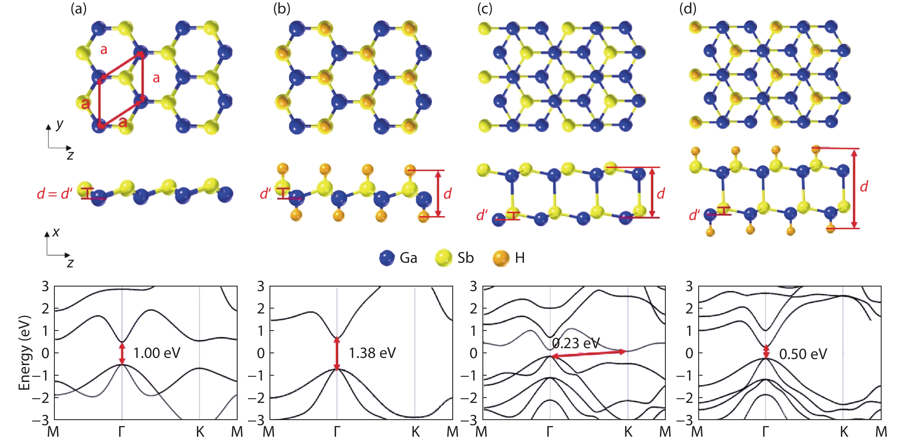
Fig. 1. (Color online) Top and side views and band structures of (a) ML GaSb, (b) ML h-GaSb, (c) BL GaSb, and (d) BL h-GaSb.
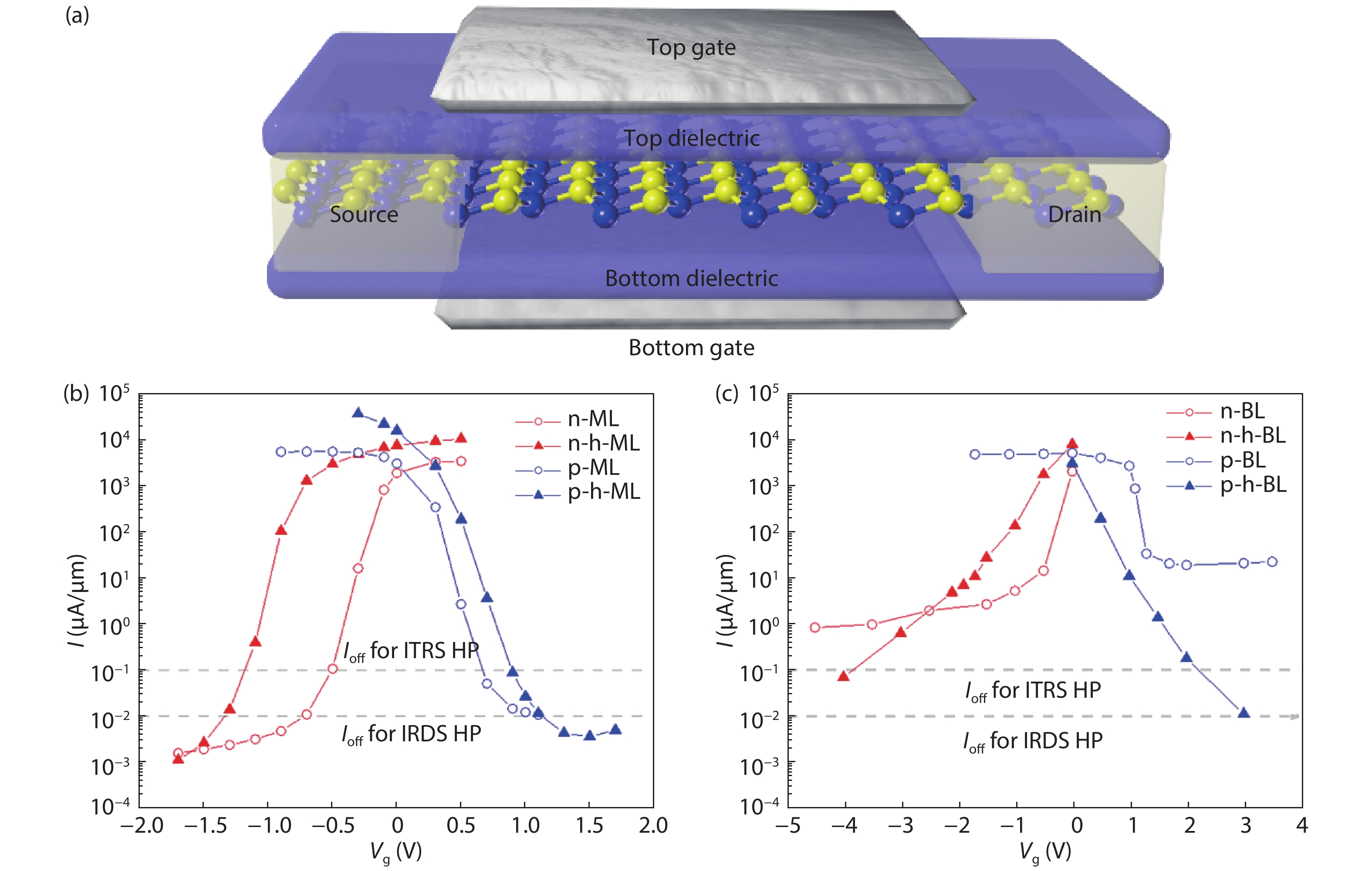
Fig. 2. (Color online) (a) Schematic model of DG ML GaSb MOSFET with 10 nm gate length. (b, c) Transfer characteristic of ML GaSb and h-GaSb and BL GaSb and h-GaSb.
Fig. 3. (Color online) (a) On-current versus the effective mass m *, (b) subthreshold swing versus transconductance, and (c) power-delay products versus delay time. Labels with and without cross-shaped subscripts represent the values calculated according to IRDS and ITRS standards, respectively. The data of other transistors with a similar gate length are also included for comparison: GaSb p-nanowire[29 ], BP (transfer along zigzag direction)[30 ], WSe2[31 ], MoS2 MOSFETs[9 ], and Si FinFET[32 ].
Fig. 4. (Color online) Position resolved local density of state and spectral current in the channel region of (a–c) ML GaSb, (d–f) ML h-GaSb and (g–i) BL h-GaSb at different states. μ s and μ d are the electrochemical potential of the source and drain, respectively. Φ B is the effective barrier height.
| ||||||||||||||||||||||||||||||||||||||||
Table 1. Structural and electronic parameters of monolayer (ML) and bilayer (BL) GaSb. h-GaSb stands for the hydrogenated layer.

Set citation alerts for the article
Please enter your email address
© Copyright 2018-2021 | Chinese Laser Press. All Rights Reserved 沪ICP备15018463号-20