
Panpan Wang, Songxuan Han, Ruge Quhe. Quantum transport simulation of the two-dimensional GaSb transistors[J]. Journal of Semiconductors, 2021, 42(12): 122001
- Journal of Semiconductors
- Vol. 42, Issue 12, 122001 (2021)
Abstract
1. Introduction
In the past few decades, the development of Si-based microelectronics obeys the performance scaling trend predicted by Moore’s law. As the building block of the microelectronics, silicon metal–oxide–semiconductor field-effect transistors (MOSFETs) behave as switches and are integrated into logic circuits to realize logic operations. Nowadays, the continuous and aggressive scaling of MOSFETs has highly increased the capability of calculation. However, traditional Si MOSFET scaling could no longer satisfy the original trend as the power density dissipated by logic chips got about 100 W/cm2[
A direct way to enhance the gate electrostatics is by decreasing the thickness of the semiconducting channel. The nature length scale λ is defined as
Most III−V semiconductors have smaller effective masses than Si, and thus higher drift velocity[
In this paper, we investigate 10 nm double-gated (DG) n- and p-type metal–oxide–semiconductor FETs with ML and bilayer (BL) GaSb by using ab initio quantum transport simulations. The DG ML GaSb MOSFETs show on-currents (Ion) ranging from 1.0 × 101 to 1.3 × 10³μA/μm. Good gate electrostatics with the subthreshold swing ranging from 87 and 120 mV/dec and transconductance from 7.9 × 10³ to 2.8 × 10⁴μS/μm are observed. The power-delay products (PDP) and delay time (τ) of almost all the studied ML GaSb MOSFETs are lower than the requirements of ITRS and IRDS, which indicates their competitiveness in low-power applications.
2. Model and method
The two-probe 10 nm-gate-length DG MOSFET is constructed with intrinsic ML and BL GaSb and their hydrogenated counterparts as the channel, respectively. The source and drain are highly doped 2D GaSb. The doping concentration is 5 × 1013 cm–2[
We apply the density functional theory (DFT) combined with the nonequilibrium Green’s function (NEGF) formalism in the Atomistix ToolKit package to calculate the electronic and transport properties[
where e is the elementary charge, h is the Planck constant, T(E, Vb, Vg) is the probability of transmission at a given gate voltage Vg and voltage Vb, fS and fD are the Fermi–Dirac distribution function for the source and drain, respectively, and μS and μD are the electrochemical potentials of the source and drain, respectively. OpenMX basis set with a mesh cut-off energy of 200 hatree was used. The temperature was set to 300 K. The Brillouin zone was sampled with separations of 0.01 Å–1[
3. Results and discussion
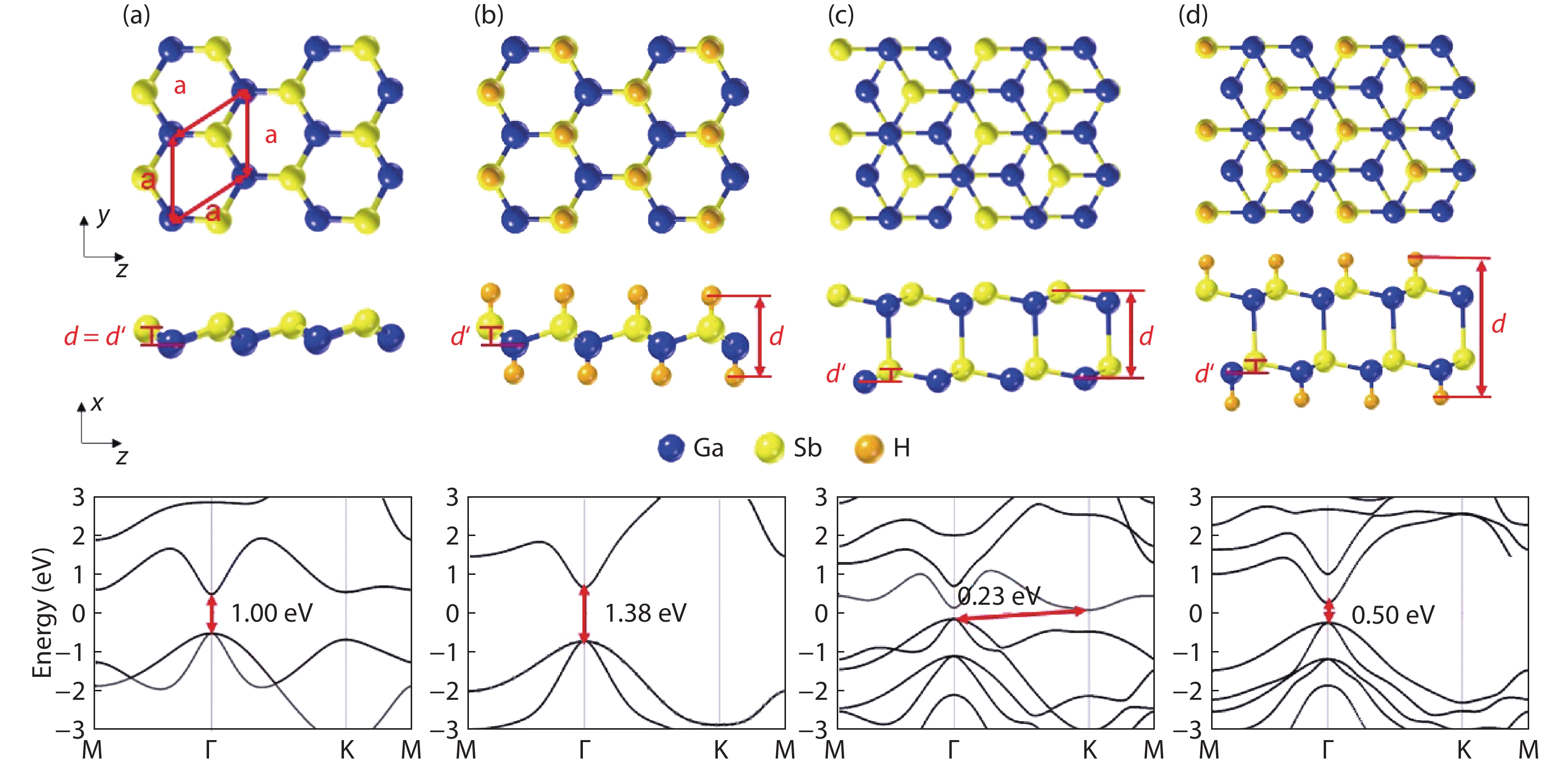
We investigate four types of GaSb-based materials: ML GaSb, BL GaSb, and their hydrogenated counterparts. The hydrogenated GaSb is noted as h-GaSb for short. These structures are shown in Fig. 1, and the optimized parameters are listed in Table 1. ML GaSb is a buckled honeycomb structure with an optimized lattice parameter of 4.36 Å and thickness of 0.80 Å. After hydrogenation, the lattice parameter of ML GaSb is slightly increased to 4.37 Å and thickness is increased to 2.19 Å. The increment of the thickness comes not only from the introduction of the H atoms, but also from the deformation of the Ga–Sb bonds. d′ is defined by the distance between two Ga and Sb atomic planes. The full hydrogenation makes Sb atom rise and Ga atom lower, increasing d′ of ML GaSb from 0.81 to 0.87 Å. It is consistent with previous theoretical studies on the ML III–V compounds[
![]()
Figure 1.(Color online) Top and side views and band structures of (a) ML GaSb, (b) ML h-GaSb, (c) BL GaSb, and (d) BL h-GaSb.
Table Infomation Is Not EnableFreestanding ML GaSb may has dangling bonds on its surface, this feature might affect the stability of the material. While there is no dangling bond on ML h-GaSb, since the surface is passivated. Comparing the phonon spectra of ML GaSb[
The electronic band structures of 2D GaSb and h-GaSb along the high symmetric k-path M–Γ–K–M are shown in Fig. 1. ML GaSb is a semiconductor with a direct bandgap of 1.00 eV. The valence band maximum (VBM) and conduction band minimum (CBM) are located at Γ point. After hydrogenating, the crystal remains a direct bandgap at Γ point with an expended size of 1.38 eV. Compared with the ML ones, the bandgaps of the BL counterparts are much smaller. BL GaSb shows an indirect bandgap of 0.23 eV with VBM located at Γ point and CBM at K point. BL h-GaSb shows a direct bandgap of 0.5 eV at Γ point. A bandgap of at least 0.4 eV is required for the semiconductor as the channel in the transistor[
The effective mass (m*) is estimated from the band structure, in accordance with the equation:
The transfer characteristics of the 2D GaSb MOSFET are shown in Figs. 2(b) and 2(c). The current of p-type devices decreases as the gate voltage increases, and the n-type ones are in contrast, which corresponds with the general trend that devices switch between the off-state and on-state. Additionally, comparing the transfer curves of the n- and p-type devices based on the same material, the ML GaSb MOSFETs have the most symmetrical current trend. The off-current (Ioff) is set to 0.1 and 0.01 μA/μm in terms of the high-performance (HP) requirement of 2015 ITRS and 2020 IRDS, respectively. From the pictures, all the devices with ML materials can meet the two requirements for Ioff, except for the BL GaSb n- and p-MOSFETs. The lowest current of BL GaSb MOSFET in the considered voltage range (–4.5 to 3.5 V) is about one or two orders of magnitude larger than 0.1 μA/μm Ioff. i.e., the BL GaSb MOSFETs are hard to turn “off”. This phenomenon is related to the small bandgap of 0.23 eV in BL GaSb. Thus, hydrogenation of the BL GaSb is suggested in order to increase the bandgap and thus suppress the source to drain leakage so that to meet the off-current requirement.
![]()
Figure 2.(Color online) (a) Schematic model of DG ML GaSb MOSFET with 10 nm gate length. (b, c) Transfer characteristic of ML GaSb and h-GaSb and BL GaSb and h-GaSb.
With Ioff = 0.1 μA/μm selected from the HP requirement of ITRS 2015 edition for 2027 horizons, Ion can be determined by the supply voltage Vdd (0.45 V): |Vg,on – Vg,off| = Vdd. Besides, from the HP standard of IRDS 2020 edition for 2028 horizons, we also calculated the Ion with 0.01 μA/μm Ioff and 0.65 V Vdd. A higher Ion indicates a faster logic transition speed of the switch. All Ion of ML GaSb and h-GaSb MOSFETs ranges from 1.0 × 101 to 1.3 × 10³μA/μm. In comparison, Ion of BL ones is lower than 1 μA/μm, which are apparently lower than most ML ones. In Fig. 3(a), we plot the on-current as a function of the effective mass in the 2D semiconductor that we considered except BL GaSb (because the simulated lowest current of the 10 nm BL GaSb MOSFET is larger than the Ioff requirement of 0.1 μA/μm). The n-MOSFETs behave better than the p-type counterparts in terms of the on-current mainly because of the much lighter effective mass. Considering materials of electron-effective masses (< 0.087m0), Ion shows an increasing trend with decreasing m* for GaSb. When heavy-hole effective masses of GaSb are relatively higher (> 0.48m0), there is no obvious dependence between Ion and effective mass. This phenomenon originates from the competition between the factors of mobility and gate controllability. While a small effective mass is beneficial for higher mobility, a larger effective mass implies a larger density of state near the Fermi level and thus better gate controllability. The latter factor becomes especially important in the ultrashort MOSFETs. As a result, no simple linear relation between the effective mass and the on-current is found. It is noted that for ML GaSb MOSFETs (no matter n- or p-type), the hydrogenation enhances the Ion of IRDS set, but ITRS ones are opposite. This may result from different slopes of transfer curves at different gate voltage range.
![]()
Figure 3.(Color online) (a) On-current versus the effective mass
It is intriguing to benchmark the performance of ML GaSb MOSFETs against transistors with other channel materials. Almost both the ML GaSb and h-GaSb MOSFETs show higher Ion than Si FinFET with a similar size of 10 nm. Compared with the 10 nm MOSFETs based on other commonly studied 2D materials like WSe2 and MoS2[
The electronic control ability of the MOSFET gate is highly significant. The subthreshold swing (SS) and transconductance (gm) evaluate the control ability in different regions. SS is a parameter describing the gate control ability at the subthreshold area. It is defined as
To understand the mechanism of gate control of MOSFETs, we calculate the local density of state for n-type DG MOSFETs with ML GaSb, ML h-GaSb, and BL h-GaSb. We define a maximum hole barrier height ΦB as the energy barrier between the highest energy level of the channel VBM and the source Fermi energy level. In Figs. 4(a)–4(c), ΦB of DG ML freestanding GaSb MOSFET is 0.78 eV when Vg = –0.9 eV at the off-state. It hinders the carrier transport from source to drain, and the current is mainly contributed by the tunneling current Itunnel. With the increase of gate voltage (–0.3 eV), the device turns to the intermediate state, and ΦB decreases to 0.32 eV. Both the tunneling current Itunnel and the thermionic current Itherm contribute significantly to the total current of 16 μA/μm. They are separated by the top of barrier height. When enhancing gate voltage to 0.3 eV, the barrier disappears, and Ion reaches 3.4 × 10³μA/μm with Itherm’s main contribution.
![]()
Figure 4.(Color online) Position resolved local density of state and spectral current in the channel region of (a–c) ML GaSb, (d–f) ML h-GaSb and (g–i) BL h-GaSb at different states.
Compared with the ML GaSb MOSFET, the ML h-GaSb MOSFET’s gate modulation (Figs. 4(d)–4(f)) is similar on the overall trend, but ΦB becomes larger in every state. From the off-state (Vg = –1.3 eV) to the intermediate-state (Vg = –0.9 eV) to the off-state (Vg = 0.3 eV), ΦB decreases from 1.69 to 0.9 and to 0 eV, and the current increases from 0.01 to 106 and to 9528 μA/μm. However, during the on-off state transition, the BL h-GaSb MOSFET (Figs. 4(g)–4(i)) performs slightly differently. Its ΦB decreases much smaller than the ML material MOSFET one. In the meantime, the current increases much smaller from 0.07 (off-state) to 0.6 (intermediate-state) and to 4.9 μA/μm (on-state). It depicts the worst control ability and the lowest switch speed among three MOSFETs.
Next, we consider the delay time (
As for radio-frequency (RF) devices, one of the most important figures of merit is the cut-off frequency (
In our simulation, SiO2 of 0.56 nm thick is used as the dielectrics. Such a thin dielectric will result in a high gate tunneling leakage current in practice. The high gate leakage will lower the circuit performance severely, and it is a critical issue especially in the sub-nanometer scale. Changing SiO2 into other high-k dielectrics such as TiO2 and HfO2 can overcome this disadvantage[
4. Conclusion
Inspired by the high mobility of III–V binary materials, we simulated the 2D GaSb n- and p-MOSFETs with a gate length of 10 nm based on ab initio quantum transport simulations. BL GaSb MOSFETs perform significantly worse than the ML ones, owing to their relatively smaller bandgap and heavier masses. Additionally, it is found that power-delay products and delay time can be best improved by about 35% and 57%, respectively, with full hydrogenation. The on-currents of ML GaSb MOSFETs range from 1 × 101 to 1.3 × 10³μA/μm, and the SS cover from 87 to 120 mV/dec. ML GaSb transistors show a fast delay time of 0.24 to 1.10 ps and low power-delay products of 0.08 to 0.45 fJ/μm. In general, the ML GaSb and h-GaSb MOSFETs perform similarly to the commonly studied ML MoS2 and WSe2 counterparts with the same gate length of 10 nm, in terms of a few figures of metrics including the on-current, PDP, and delay time. Therefore, making GaSb thinner, ideally fabricating the thinnest ML GaSb, is worthy of being tested for the ultrashort transistors in the experiment.
Acknowledgements
This work was supported by the National Natural Science Foundation of China (No. 91964101), the Fund of State Key Laboratory of Information Photonics and Optical Communications (Beijing University of Posts and Telecommunications) and the Research Innovation Fund for College Students of Beijing University of Posts and Telecommunications.
References
[1] D J Frank. Power-constrained CMOS scaling limits. IBM J Res Dev, 46, 235(2002).
[2] R H Yan, A Ourmazd, K F Lee. Scaling the Si MOSFET: From bulk to SOI to bulk. IEEE Trans Electron Devices, 39, 1704(1992).
[3] C Hu. FinFET and UTB: How to make very short channel MOSFETs. ECS Trans, 50, 17(2013).
[4]
[5] K Uchida, H Watanabe, A Kinoshita et al. Experimental study on carrier transport mechanism in ultrathin-body SOI nand p-MOSFETs with SOI thickness less than 5 nm. Dig Int Electron Devices Meet, 47(2002).
[6] K Uchida, H Watanabe, J Koga et al. Experimental study on carrier transport mechanism in ultrathin-body SOI MOSFETs. International Conference on Simulation of Semiconductor Processes and Devices, 8(2003).
[7] D A Bandurin, A V Tyurnina, G L Yu et al. High electron mobility, quantum Hall effect and anomalous optical response in atomically thin InSe. Nat Nanotechnol, 12, 223(2017).
[8] L K Li, Y J Yu, G Ye et al. Black phosphorus field-effect transistors. Nat Nanotechnol, 9, 372(2014).
[9] B Radisavljevic, A Radenovic, J Brivio et al. Single-layer MoS2 transistors. Nat Nanotechnol, 6, 147(2011).
[10] F Schwierz, J Pezoldt, R Granzner. Two-dimensional materials and their prospects in transistor electronics. Nanoscale, 7, 8261(2015).
[11] L Tao, E Cinquanta, D Chiappe et al. Silicene field-effect transistors operating at room temperature. Nat Nanotechnol, 10, 227(2015).
[12] A Acun, B Poelsema, H J W Zandvliet et al. The instability of silicene on Ag(111). Appl Phys Lett, 103, 263119(2013).
[13] G Doornbos, M Passlack. Benchmarking of III–V n-MOSFET maturity and feasibility for future CMOS. IEEE Electron Device Lett, 31, 1110(2010).
[14] J A del Alamo, D A Antoniadis, J Q Lin et al. Nanometer-scale III-V MOSFETs. IEEE J Electron Devices Soc, 4, 205(2016).
[15] X Lü, S S He, H X Lian et al. Structural, electronic, and optical properties of pristine and bilayers of hexagonal III-V binary compounds and their hydrogenated counterparts. Appl Surf Sci, 531, 147262(2020).
[16] H Riel, L E Wernersson, M Hong et al. III-V compound semiconductor transistors — from planar to nanowire structures. MRS Bull, 39, 668(2014).
[17] B P Bahuguna, L K Saini, R O Sharma et al. Strain and electric field induced metallization in the GaX (X = N, P, As & Sb) monolayer. Physica E, 99, 236(2018).
[18] T Low, A S Rodin, A Carvalho et al. Tunable optical properties of multilayer black phosphorus thin films. Phys Rev B, 90, 075434(2014).
[19] M Brandbyge, J L Mozos, P Ordejón et al. Density-functional method for nonequilibrium electron transport. Phys Rev B, 65, 165401(2002).
[20] J M Soler, E Artacho, J D Gale et al. The SIESTA method for ab initio order-
[21] H J Monkhorst, J D Pack. Special points for Brillouin-zone integrations. Phys Rev B, 13, 5188(1976).
[22] J P Perdew, K Burke, M Ernzerhof. Generalized gradient approximation made simple. Phys Rev Lett, 77, 3865(1996).
[23] H L Zhuang, A K Singh, R G Hennig. Computational discovery of single-layer III-V materials. Phys Rev B, 87, 165415(2013).
[24] X F Fan, W T Zheng, J L Kuo et al. Structural stability of single-layer MoS2 under large strain. J Phys: Condens Matter, 27, 105401(2015).
[25] S S Lin. Light-emitting two-dimensional ultrathin silicon carbide. J Phys Chem C, 116, 3951(2012).
[26] A K Singh, H L Zhuang, R G Hennig. Ab initiosynthesis of single-layer III-V materials. Phys Rev B, 89, 245431(2014).
[27] F Schwierz. Graphene transistors. Nat Nanotechnol, 5, 487(2010).
[28] D M Riffe. Temperature dependence of silicon carrier effective masses with application to femtosecond reflectivity measurements. J Opt Soc Am B, 19, 1092(2002).
[29] D Yadav, D R Nair. Impact of source to drain tunneling on the ballistic performance of Si, Ge, GaSb, and GeSn nanowire p-MOSFETs. IEEE J Electron Devices Soc, 8, 308(2020).
[30] R G Quhe, X Y Peng, Y Y Pan et al. Can a black phosphorus Schottky barrier transistor be good enough. ACS Appl Mater Interfaces, 9, 3959(2017).
[31] X T Sun, L Xu, Y Zhang et al. Performance limit of monolayer WSe2 transistors; significantly outperform their MoS2 counterpart. ACS Appl Mater Interfaces, 12, 20633(2020).
[32] B Yu, L Chang, S Ahmed et al. FinFET scaling to 10 nm gate length. IEEE International Electron Devices Meeting, 251(2002).
[33] Z Y Ni, M Ye, J H Ma et al. Performance upper limit of sub-10 nm monolayer MoS2 transistors. Adv Electron Mater, 2, 1600191(2016).
[34] B R Bennett, M G Ancona, J B Boos et al. Strained GaSb/AlAsSb quantum wells for p-channel field-effect transistors. J Cryst Growth, 311, 47(2008).
[35] B R Bennett, T F Chick, M G Ancona et al. Enhanced hole mobility and density in GaSb quantum wells. Solid State Electron, 79, 274(2013).
[36] Y W Chen, Z Tan, L F Zhao et al. Mobility enhancement of strained GaSb p-channel metal–oxide–semiconductor field-effect transistors with biaxial compressive strain. Chin Phys B, 25, 038504(2016).
[37] J A del Alamo. Nanometre-scale electronics with III-V compound semiconductors. Nature, 479, 317(2011).
[38] A Bansal, B C Paul, K Roy. Modeling and optimization of fringe capacitance of nanoscale DGMOS devices. IEEE Trans Electron Devices, 52, 256(2005).
[39] J Lacord, G Ghibaudo, F Boeuf. Comprehensive and accurate parasitic capacitance models for two- and three-dimensional CMOS device structures. IEEE Trans Electron Devices, 59, 1332(2012).
[40] L Wei, F Boeuf, T Skotnicki et al. Parasitic capacitances: Analytical models and impact on circuit-level performance. IEEE Trans Electron Devices, 58, 1361(2011).
[41] L Vicarelli, M S Vitiello, D Coquillat et al. Graphene field-effect transistors as room-temperature terahertz detectors. Nat Mater, 11, 865(2012).
[42] S Singh, K Thakar, N Kaushik et al. Performance projections for two-dimensional materials in radio-frequency applications. Phys Rev Appl, 10, 014022(2018).
[43] S Prasanna Kumar, P Sandeep, S Choudhary. Changes in transconductance (

Set citation alerts for the article
Please enter your email address
© Copyright 2018-2021 | Chinese Laser Press. All Rights Reserved 沪ICP备15018463号-20