Key Laboratory of Photoelectron Imaging Technology and System of the Ministry of Education, School of Optics and Photonics, Beijing Institute of Technology, Beijing 100081, China
Shanshan Mao, Yanqiu Li, Jiahua Jiang, Shihuan Shen, Ke Liu, Meng Zheng. Design of a hyper-numerical-aperture deep ultraviolet lithography objective with freeform surfaces[J]. Chinese Optics Letters, 2018, 16(3): 030801
Copy Citation Text
We have proposed and developed a design method of a freeform surfaces (FFSs) based hyper-numerical-aperture deep ultraviolet (DUV) projection objective (PO) with low aberration. With an aspheric initial configuration, lens-form parameters were used to determine the best position to remove elements and insert FFSs. The designed FFSs PO reduced two elements without increasing the total thickness of the glass materials. Compared with aspheric initial configuration, the wavefront error of the FFSs PO decreased from to , the distortion reduced from 1 to 0.5 nm, and the aspheric departure decreased from 1.7 to 1.35 mm. The results show that the design method of the FFSs PO is efficient and has improved the imaging performance of PO. The design method of FFSs PO provides potential solutions for DUV lithography with low aberrations at 10–5 nm nodes.
The projection objective (PO) is a key component of deep ultraviolet (DUV) lithography tools[1,2]. For 22–14 nm technology nodes, a hyper-numerical-aperture (NA) PO adopts aspheric surfaces (ASPSs)[3]. When the resolution is decreased to 10–5 nm nodes, a stricter wavefront error (root mean square, ) is required[4]. Aspheric PO needs to use numerous lenses to correct aberrations, and it increases the dimension and total track of the design significantly. Adopting freeform surfaces (FFSs) in a lens system is a potential means to enhance performance and achieve a compact lens design. In an objective with a given number of elements, using FFSs can further increase the image NA or exposure field, so an FFSs PO has the potential to achieve higher resolution[5,6]. These advantages of FFSs are highly useful for off-axis head-mounted display imaging systems to enlarge the field of view and decrease the F-number or for on-axis imaging applications with high aspect ratios to provide solutions with a clearly better overall imaging performance[7–9]. Therefore, it is necessary to investigate and explore a novel design of FFSs hyper-NA PO to meet the requirements of the next node DUV lithography.
An FFSs catadioptric PO for lithography with NA 0.8 was designed by Mann[10]. However, he did not describe the specific design methods of the FFSs PO, and whether the designed PO has the potential to meet lithography requirements is unknown. In terms of optical system evaluation parameters, Sasian and Descour proposed two lens-form parameters ( and ) to design an NA 0.38 spherical PO; the two parameters quantify the symmetry of the objective and the optical power distribution among the individual optical elements[11]. With these two parameters as criteria, Cheng et al. established a mechanism for automatically identifying addition and deletion elements during optimization[12]. Sasian and Cheng have designed spherical POs with small NAs, which cannot meet the requirements of current and subsequent nodes. Therefore an FFSs hyper-NA PO needs to be explored to meet 10–5 nm technology nodes. However, few design methods for the FFSs PO with a hyper-NA have been proposed in the past, so it has been a challenge to design an FFSs PO that has low aberration, while maintaining a hyper-NA with a compact structure.
In this Letter, we investigate and utilize lens-form parameters to design an FFSs hyper-NA PO. The lens-form parameters ( and ) are used to determine the best position to remove elements and insert FFSs. Design efficiency was greatly improved when this approach was used compared with the traditional experience and the trial-and-error method. Combining with a gradual optimization strategy, an NA 1.2 FFSs PO with low aberration and distortion was designed. The designed FFSs PO reduced two elements without increasing the total thickness of the glass materials. Compared with aspheric initial configuration, the wavefront RMS error of the FFSs PO decreased from to . The design results proved the effectiveness of the proposed method. The multi-patterning methods and multiple mask-split/multi-exposure/etch sequences were used in ASML’s TWINSCAN NXT: 1970 Ci lithography tool with variable NAs (0.85–1.35) to support a sub 20 nm node[13]. The designed 1.2 NA FFSs PO with these resolution enhancement technologies provides valuable support for 10–5 nm technology nodes.
Sign up for Chinese Optics Letters TOC. Get the latest issue of Chinese Optics Letters delivered right to you!Sign up now
The Letter is organized as follows: (1) the lens-form parameters ( and ) and the gradual optimization strategy are defined and illustrated in the design process. (2) An aspheric initial configuration satisfying the basic requirements of the lithography objective was selected and optimized to achieve high (diffraction limited) image quality. (3) The lens-form parameters ( and ) were used to determine the best position to remove elements, and the saddle point construction method was used to perform the removal process. (4) After element deletion, when image quality degradation was unacceptable, FFSs were inserted to the obtained system to improve imaging performance. The positions of the inserted FFSs were determined by the same method based on lens-form parameters.
The two lens-form parameters ( and ) quantify the symmetry of the optical system and the optical power distribution among individual elements, so they can be used to determine the most appropriate position to remove elements and insert FFSs. According to paraxial marginal and chief ray tracing, the lens-form parameters are independent of lens dimension, aperture size, field angle, or surface shape[11].
The first parameter is optical power parameter . It evaluates the distribution of optical power and is derived from the square root of the averaged and squared weighted refracted powers, , of the lens surfaces: where is the total number of surfaces. is the weighted refractive power of surface , the expression of which is described below: where is the magnification of the entire system; is the marginal paraxial ray height on surface ; is the product of the index of refraction and marginal paraxial ray slope in image space; and are the indices of refraction before and after the th surface, respectively; and is the surface radius.
The second parameter is symmetric degree parameter . It evaluates the symmetric degree of the objective surfaces, and it is the extent to which surfaces are concentric to the stop or satisfy the aplanatic condition. The equation is where is written as
In the expression above, is the product of refractive index and the paraxial chief ray angle of incidence on surface ; is the value of at the stop surface; and and are the paraxial marginal ray slope before and after surface , respectively.
According to the definition of ,
The result shows that a surface with a large contributes much to the total optical power of the system. When the values of are equal, is minimized. Every optical surface contributes equally to the lens power. It has demonstrated that objectives with small values of and have a large imaging potential[11].
() contains the lens-form parameters of a surface. The lens-form parameter of an element is defined as (). An element with small and values contributes little to the total optical power and symmetry of the objective. When the element is removed, image quality is not seriously damaged. When a new surface or element is inserted at the surface with the largest or it would take up some stress optical power concentrated in the area or improve the symmetry of the system. This results in improved performance of the objective. The usage is illustrated in Table 1.
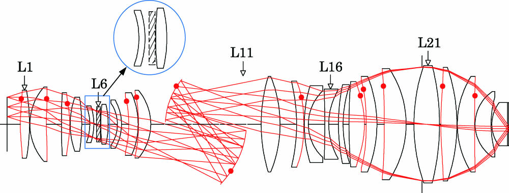
As revealed by the example in Fig. 1, an aspheric PO with NA 1.2 consists of 25 optical elements[14].The value of was 0.1479, and the value of was 0.4458. The optical characteristics are shown in Table 2.
Figure 1.Layout of the initial aspheric PO. The red dots represent aspheric surfaces.
To evaluate the aberration correction potential of the aspheric PO with reduced lenses, we removed elements from the aspheric PO in Fig. 1. Thus, the lens with the smallest or may be removed.
Figure 2.Lens-form parameters of a single element in aspheric PO: (a) value of a single element and (b) value of a single element.
As shown in Fig. 2, the sixth element () is the most appropriate to delete. The saddle point construction method was used to remove the sixth lens[15]. The obtained aspheric PO structure is shown in Fig. 3. Its structure has not changed significantly, and the error function can converge to a small value. The wavefront RMS error is (), and the distortion is less than 1.5 nm, which means the system still presents a promising imaging performance. Therefore, additional elements can be removed.
Figure 3.Aspheric PO structure after removing one element.
The lens-form parameters of each element in the structure in Fig. 3 were evaluated again. The result shows the 13th and 1st elements provide small contribution to the total optical power; their values are 0.0329 and 0.0318, respectively. However, the first element plays an important role in keeping telecentricity at the mask side and should not be removed. Therefore, we removed the 13th element. However, the rear surface of the 13th element is an ASPS that undertakes correction of a large number of residual aberrations. To make up the aberration correction capability, an ASPS was added near the position of the removed 13th element.
After gradual optimization, the aspheric PO structure with two lenses removed is shown in Fig. 4. The edge thicknesses of several positive lenses are very small and tend to become negative. Figure 5 shows the aspheric PO sampled fields and the footprint map. As shown in the footprint map in Fig. 5(b), vignetting is generated at the edge of field 7. The capability to correct aberrations is weakened because two elements were removed. To compensate for the aberration correction capability, single lens surface power was strained. Optical power cannot be reasonably distributed under such strict structure constraints, which cause aspheric PO deformation and vignetting. Given that vignetting is not allowed in lithography, freedom degrees have to be increased to assure that all light originating at the mask reaches the wafer.
Figure 4.Aspheric PO structure after removing two elements.
At this point, the system wavefront RMS error is (), and the distortion is 8.7 nm. The optical power parameter is 0.1509, and the symmetry parameter is 0.4170. The decreased symmetry parameter shows that the symmetry of the PO remains good; the increased optical power parameter indicates that a single lens optical power has not been effectively used.
The surface we used for the design purpose is the 10th even terms polynomial-based surface. Sampled fields were shown in Fig. 6, and 16 field points are selected in the first quadrant.
The position of the FFS affects the performance of the objective significantly. Even when the same number of FFSs is used, the effect of FFSs differs depending on their positions. The rays passing through the stress surfaces produce large deflections, and a large number of high-order aberrations are generated on these surfaces. We added the FFSs at these positions to enhance the correction capability for high-order aberrations and alleviate the optical power strain.
To improve optimization efficiency, the positions for adding FFSs were selected from the existing aspheric positions. For the objective structure in Fig. 4, the resulting contribution values are listed in descending order in Table 1. ASPS 30 (largest value of ) was fitted to the FFS. After gradual optimization, the distortion value was reduced to 2.5 nm, whereas the wavefront RMS error was nearly unchanged. To reduce the aberrations, more FFSs were added continuously.
Surface No.
wj
Surface No.
sj
S30
0.3071
S30
0.9891
S20
0.2472
S20
0.9363
S19
0.1918
S1
0.5773
S15
0.1334
S15
0.4754
S23
0.1301
S17
0.3222
S38
0.0519
S41
0.3073
S17
0.0485
S19
0.2142
S1
0.0372
S4
0.2090
S6
0.0312
S23
0.1843
S4
0.0162
S6
0.1601
S41
0.0161
S31
0.1447
S33
0.0149
S38
0.1168
S31
0.0050
S33
0.0618
Table 1. Lens-form Parameter Values of Aspheric Surfaces
After evaluating lens-form parameters, two aspheric mirrors, S20 and S19, contribute the most to the optical power. However, the sensitivity of the mirror is two times that of the refractive one because of twice deflection. To make the PO stable, we fit the refractive ASPS S15 to a freeform one. Then, S20 and S19 were replaced by FFSs successively. Combining with a gradual optimization, a high-image-quality FFSs PO was achieved in Fig. 7. The optical characteristics of the FFSs PO are described in Table 2. The modulation transfer function (MTF) plot is shown in Fig. 8. Image resolution already reached the diffraction limit. The footprint map in Fig. 9 shows that the FFSs PO shows no vignetting. In Fig. 10(a), the wavefront RMS error is less than (). In Fig. 10(b), the distortion in the full image field is controlled to less than 0.5 nm. At the same time, the two lens-form parameters are reduced, the value of optical power parameter is 0.1481, and the value of symmetry parameter is 0.3971.
Item
ASPSs PO
FFSs PO
Numerical aperture
1.2
1.2
Wavelength
193 nm
193 nm
Image-side field of view
26mm×5.5mm
26mm×5.5mm
Magnification
0.25
0.25
Front working distance
33 mm
33 mm
Total track length
1253 mm
1232 mm
Number of aspheric surfaces
13
9
Number of freeform surfaces
4
Number of lenses
25
23
Thickness of all lenses
659 mm
631 mm
Telecentricity
<6mrad
<6mrad
Max. aspheric departure
<1.7mm
<1.35mm
Wavefront RMS error
<0.006λ
<0.005λ
Distortion
<1nm
<0.5nm
Table 2. Optical Characteristics of ASPSs and FFSs POs
Compared with the TWINSCAN XT: 1700i lithography tool that ASML has manufactured, its PO has an NA 1.2 at 193 nm wavelength, and a scanning field. The wavefront RMS error is 1.4 nm, and the distortion is 5 nm[16]. The designed hyper-NA FFSs PO has better wavefront error and distortion values than the above with the same NA, wavelength, and scanning field.
The manufacturability of the ASPSs and the FFSs, was evaluated. The maximum aspheric departure is 1.35 mm. The maximum local curvature of the FFSs in the and directions is 0.0053, as shown in Fig. 11(d). Compared with the previous FFSs that were fabricated[17], the FFSs in this PO possess proper local curvatures and gentle shapes. Therefore, we conclude that the surfaces in the FFSs PO are reasonable.
Figure 11.Local curvature of FFSs in the and directions. Only the used area of each surface is shown. (a) S16; (b) S21; (c) S22; (d) S33.
In conclusion, lens-form parameters and a gradual optimization strategy were used to design an FFSs hyper-NA PO. With the presented method, an NA 1.2 FFSs PO was designed. By adding four freeform surfaces at the positions determined by the lens-form parameters, two elements were removed from the PO. The wavefront RMS error reaches , and the distortion is less than 0.5 nm. The maximum aspheric departure is reduced from 1.7 to 1.35 mm. The results show that our method provides an effective approach to designing the FFSs PO and provides valuable support for 10–5 nm nodes.
Shanshan Mao, Yanqiu Li, Jiahua Jiang, Shihuan Shen, Ke Liu, Meng Zheng. Design of a hyper-numerical-aperture deep ultraviolet lithography objective with freeform surfaces[J]. Chinese Optics Letters, 2018, 16(3): 030801