
Binze Zhou, Mengjia Liu, Yanwei Wen, Yun Li, Rong Chen. Atomic layer deposition for quantum dots based devices[J]. Opto-Electronic Advances, 2020, 3(9): 190043-1
- Opto-Electronic Advances
- Vol. 3, Issue 9, 190043-1 (2020)
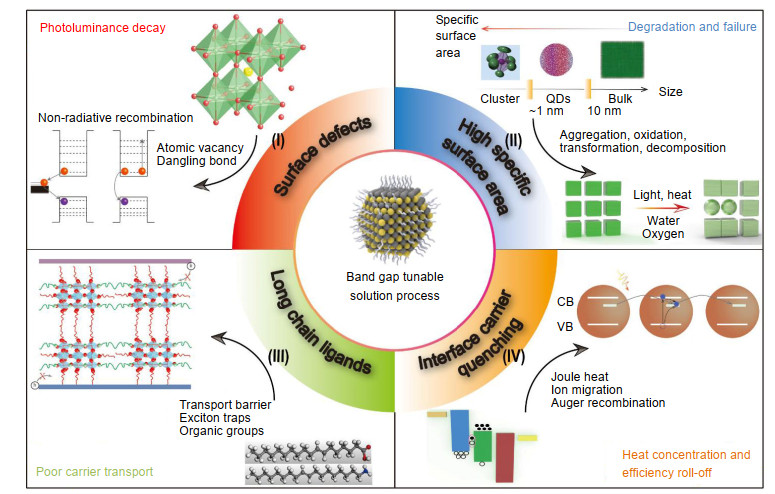
Fig. 1. The corresponding challenges of QDs.
(I ) Non-radiative recombination corresponding to photoluminance decay. (Ⅱ ) High specific surface area corresponding to degradation and failure. (Ⅲ ) Long chain ligands corresponding to poor carrier transport. (Ⅳ ) Interfacial carrier accumulation and recombination corresponding to heat and efficiency roll-off.
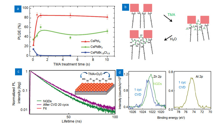
Fig. 2. (a ) PLQY value variation of QDs with TMA treatment time75. (b ) Reaction schematic of TMA with QDs surface75. (c ) PL lifetimes of QDs thin films before and after 20 cycles of alumina deposition69. (d ) XPS spectra of Zn for QDs thin film before and after one cycle of alumina and Al after one cycle of alumina69. Figure reproduced from: (a, b) ref.75, Creative Commons Attribution 2.0 International License; (c, d) ref.69, American Chemical Society.
Fig. 3. (a ) Cross-sectional TEM structure characterization and optical absorption spectra stability test before and after ALD treatment74. (b ) EELS color-coded elemental intensity maps of Al and Br, CsPbBr3 QD/AlOx nanocomposites PL properties over 45 days of storage in ambient conditions and after 1 h of soaking in water70. Figure reproduced from: (a) ref.74, American Chemical Society; (b) ref.70, John Wiley and Sons.
Fig. 4. (a ) Schematic of device architecture, FET electron mobility (black) and threshold voltage (blue) as a function of time stored and operated in air86. (b ) TEM image of device structure and the relative power conversion efficiency (PCE) over time84. Figure reproduced from: (a) ref.86, American Chemical Society; (b) ref.84, AIP Publishing.
Fig. 5. (a ) FTIR spectra of ALD-coated and uncoated thin films comprised of ZnO nanocrystals76. (b ) XPS scans for Pb 4f and Al 2p of the Alx Oy -PbS film78. (c ) Ligands exchange and ALD infilling schematic resulting in barrier width and height reduce55. Figure reproduced from: (a) ref.76, American Chemical Society; (b) ref.78, AIP Publishing; (c) ref.55, American Chemical Society.
Fig. 6. (a ) Schematic of barrier layer configurations available in quantum dot-sensitized solar cells. Comparison of device efficiency and dark current onset for TiO2/Al2O3/QD and TiO2/QD/Al2O3 configurations under 1 sun of illumination with varying ALD cycles of Al2O382. (b ) Band energy level diagram of each material in QLED. Current density of electron only device without and with Al2O3 interlayers, and hole only device. Device lifetime of QLEDs without and with Al2O3 interlayer63. Figure reproduced from: (a) ref.82, American Chemical Society; (b) ref.63, Creative Commons Attribution 3.0 International License.
Fig. 7. (a ) Schematic diagram of the ALD interface passivating mechanism61. (b ) EDS mappings obtained after device operation for QLEDs without and with an Al2O3 barrier layer61. Figure reproduced from ref.61, American Chemical Society.
|
Table 1. Summary of ALD systems reported in literature for applications in QDs and QDs based devices

Set citation alerts for the article
Please enter your email address
© Copyright 2018-2021 | Chinese Laser Press. All Rights Reserved 沪ICP备15018463号-20