Abstract
Quantum dots (QDs) are promising candidates for the next-generation optical and electronic devices due to the outstanding photoluminance efficiency, tunable bandgap and facile solution synthesis. Nevertheless, the limited optoelectronic performance and poor lifetime of QDs devices hinder their further applications. As a gas-phase surface treatment method, atomic layer deposition (ALD) has shown the potential in QDs surface modification and device construction owing to the atomic-level control and excellent uniformity/conformality. In this perspective, the attempts to utilize ALD techniques in QDs modification to improve the photoluminance efficiency, stability, carrier mobility, as well as interfacial carrier utilization are introduced. ALD proves to be successful in the photoluminance quantum yield (PLQY) enhancement due to the elimination of QDs surface dangling bonds and defects. The QDs stability and devices lifetime are improved greatly through the introduction of ALD barrier layers. Furthermore, the carrier transport is ameliorated efficiently by infilling interstitial spaces during ALD process. Attributed to the ultra-thin and dense coating on the interface, the improvement on optoelectronic performance is achieved. Finally, the challenges of ALD applications in QDs at present and several prospects including ALD process optimization, in-situ characterization and computational simulations are proposed.Introduction
Quantum dots (QDs) are typical semiconductor nanocrystals which exhibit tunable bandgap, excellent photoluminance efficiency and high extinction coefficient1-3. The optoelectronic performance can be tailored by the size, shape, and composition as well as the surface structure of QDs due to the quantum confinement on the nanoscale. Moreover, the overall physical peculiarity of QDs can be designed by selecting the characteristics of the individual QD building block and by controlling the electronic communication between the QDs in the solid state. Thus, they have been widely used in the fields of photodetectors4-6, photovoltaics7-9, light-emitting diodes (LED)10-12 and field-effect transistor (FET)13.
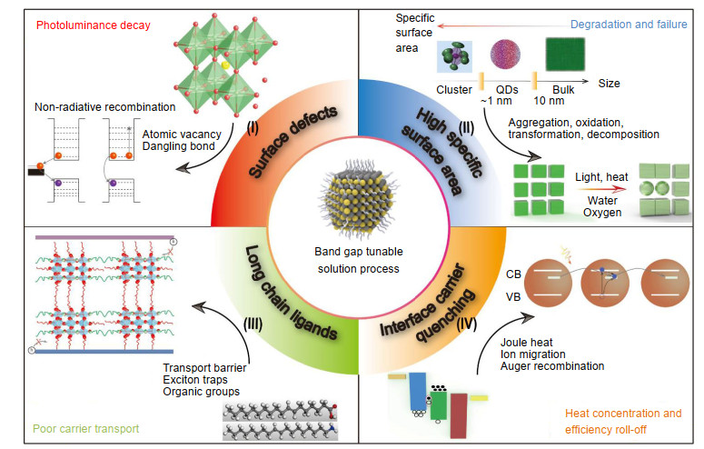
Although QDs have excellent optoelectronic properties, several issues remain to be addressed as shown in Fig. 1. The photoluminance quantum yield (PLQY) of QDs is seriously limited by surface trap-states which are originated from the dangling bonds and atomic vacancy14, as shown in Fig. 1(Ⅰ). They act as the non-radiative recombination centers and reduce the fluorescence quantum yield seriously15, 16. Moreover, the large specific surface area and under-coordinated sites make QDs vulnerable to water/oxygen/photo/heat, which may change their original size, component and crystal structure17 (Fig. 1(Ⅱ)). On device level, the poor carrier transport of QDs solids film caused by long-chain organic ligands and carrier recombination loss at interface between different functional layers severely influence the optoelectronic performance of the QDs device18, as indicated from Fig. 1(Ⅲ) & (Ⅳ). As a result, the low optoelectronic efficiency and short lifetime become stumbling blocks for further applications of QDs optoelectronic devices.

Figure 1.The corresponding challenges of QDs.
(I) Non-radiative recombination corresponding to photoluminance decay. (Ⅱ) High specific surface area corresponding to degradation and failure. (Ⅲ) Long chain ligands corresponding to poor carrier transport. (Ⅳ) Interfacial carrier accumulation and recombination corresponding to heat and efficiency roll-off.
To address these concerns, strategies to modify the structures of the QDs based devices were proposed from different aspects. Long-chain ligands and core-shell structures were commonly used to improve the PLQY and surface stability of QDs19, 20. The introduction of long-chain ligands was able to passivate the under-coordinated atoms on the surface and maintained a high dispersion stability of colloidal QDs in solution. Core-shell structure could confine wave function of the QDs in a limited region, and prevent the ambient environmental invasion, such as oxygen and water21-24. Embedding QDs into other matrix such as polymer, oxide or inorganic salts achieved similar protection effect25. Nevertheless, long-chain organic ligands and core-shell structures also blocked the carrier transport among QDs and the carrier injection into QDs, leading to poor carrier mobility25. Ligands exchange with shorter ones was utilized to enhance carrier transport, and the device performance proved to be greatly improved26-28. Besides, for QDs-based devices, the misalignment of energy level between different functional layers would lead to the imbalance of the carrier concentration and the increase of Auger recombination29, 30. By introducing functional layers into QDs-based devices, the non-radiative recombination between QDs and other functional layers were effectively eliminated. As a result, photoelectric efficiency roll-off was suppressed31-33.
As an atomic scale controllable surface treatment technique, atomic layer deposition (ALD) meets the above requirements of QDs based device fabrications and has been successfully used in the modification of QDs and QDs-based devices34, 35. ALD is a gas phase deposition method relying on a sequence of self-limiting surface reaction steps to deposit ultrathin, uniform and conformal films36. ALD has been extensively implemented into semiconducting processes in the past decade37, 38. It is suitable to grow high-quality dielectric and semiconductor on different substrate even including the porous and high-aspect ratio substrates39-42, which has been widely used in areas of thin film solar cell, photodetectors and other electronic devices43-46. Besides, ALD is also a powerful method in thin film encapsulations for flexible electronics, due to the advantages of free pin-hole, excellent conformality and precise nanoscale thickness control on large area47-49. It is decent for surface defects passivation, dense thin film encapsulation, interstitial infilling and interface functional layers fabrication due to the characteristics of energy-dependent self-limiting reactions, dense uniform thin film fabrication, gas-phase infiltration and atomic level thickness control.
In this perspective, the relevant works of ALD modification on QDs are summarized in Table 1. From the aspect of modified objects, ALD is mainly used to modify the Ⅱ-Ⅵ (Ⅳ-Ⅵ) groups QDs and has been extended to perovskite QDs based devices recently. The ALD modified QDs have found applications in luminescence, displays, photovoltaics, and field effect transistors. The ALD grown materials used for QDs modification are mainly concentrated to the inorganic oxides such as Al2O3, ZnO and TiO2. As for the ALD process for QDs modification, there are two issues needed to be addressed including temperature and pulse/purge time. Because of the sensitivity and vulnerability of QDs to the temperature, the deposition temperature must be relatively low. Meanwhile, a temperature too low may induce porous structure, which affects the moisture resistance of the film. On the other hand, the pulse time needs to meet the requirements of surface chemical and physical saturation absorption for next-step half reaction. The purge time should be minimized while ensuring that the residue is cleaned out at the same time. In this perspective, we focus on the ALD modifications rather than the growth of QDs, although literatures have shown the capacity of ALD on adjusting QDs size and making core-shell structures50-52.
| ALD materials | Precursors | Temperature (℃)
| QDs | QDs applications |
| ZnO53-60 | DEZ (Diethyl Zinc)+O253DEZ+H2O54-59 | 27–7555, 7557, < 10060, 10054, 15056, 18058, 20059, 22053 | ZnO58PbS56PbSe55, 57CdSe53, 54CdSe/CdS/ZnS59CsPbBr360 | Film53, 54, 57-59FET55 Solar cell55, 56LED60 |
| Al2O345, 46, 55-58, 60-91 | TMA (Trimethyl Aluminum)
+H2O55-57, 61, 62, 65-70, 72-74, 76, 77, 79-89TMA+O2 plasma88TMA+Air75, 91TMA+O271TMA+N2O plasma63 | 18 ± 175, 27–755527–12583, 2774, 80, 895070, 30–180737078, 75578062, 63, 84, 8779< 10060, 10069, 81, 1106615056, 61, 67, 68, 72, 8716085, 17582, 1805819077, 20088, 25086 | ZnO58, 76CdTe73, CdS82CdSe86, 88CdSe/ZnS61, 66, 77, 87ZnCdSSe/ZnS68CdSe@ZnS/ZnS63CdSe/CdS/ZnS69, 71PbS56, 67, 72, 78, 81, 83-85, 89PbSe55, 57, 74, 79, 80APbX360, 65, 70, 75 | Sphere65Film57, 58, 66, 69, 70, 73, 74, 77FET55, 62, 76, 78-80, 83, 86, 88Solar cell56, 82, 84, 85Photodetector67, 81Photocatalysis72LED60, 61, 63, 68, 71, 75, 87, 91 |
| TiO262, 92-94 | Ti(OiPr)4 (Titanium isopropoxide)+H2O92, 93TDMAT(Tetrakis(dimethylamido)titanium)
+H2O62, 94 | 8062, 15094, 20092, 93 | CdS92-94CdSe/CdS/ZnS62 | Film62Solar cell92, 93Photocatalysis94 |
| ZrO284 | TDMA-Zr(Tetrakis(dimethylamido)zirconium)+H2O84 | 8084 | PbS84 | Solar cell84 |
| HfO262, 76, 79 | TDMAH(Tetrakis(dimethylamino)hafnium)+H2O76, 79TEMAHf(Tetrakis(ethylmethylamino)hafnium)+O362 | 7576, 8062, 8779 | ZnO76CdSe/CdS/ZnS62PbSe79 | Film62, 76FET79 |
| ZnS62 | DEZ+H2S62 | 8062 | CdSe/CdS/ZnS62 | Film62 |
| AlN95 | TMA+ H2/N2/Ar plasma95 | 150, 20095 | CdSexTe1−x95 | Solar cell95 |
Table 1. Summary of ALD systems reported in literature for applications in QDs and QDs based devices
The enhancement of the PLQY by defects elimination methods such as elective curing on dangling bonds and oxidation of defects sites is first presented. Ultra-thin films obtained by ALD are dense and pinhole-free, which act as ideal barrier layers to prevent ambient environmental invasion and suppress ion migration. The stability of QDs devices is also improved by such process. Besides, the original carrier mobility is improved by ALD passivation. The electronic traps density and carrier transport barrier were significantly reduced due to the infilling into the inter-dot gaps by ALD. In terms of interface engineering for carriers' efficient utilization, the effectiveness of ALD's aligned energy level and dense insulation layer on carrier recombination suppression and ion migration inhibition is discussed in details. At the end, prospects of ALD applications on QDs based devices are discussed from the aspects of ALD materials, process parameters, in-situ characterization and device simulations.
ALD applications for QDs-based devices
Photoluminance enhancement
As the basic building blocks of QDs based devices, excellent photoluminance of QD monomers is crucial to achieve high-performance QDs-based optoelectronic devices. However, the PLQY of QDs is sensitive to their surface atomic states where severe excitons quenching takes place. It is known that the dangling bonds and atomic vacancy may introduce obvious mid-gaps states inside the band gap of QDs which serve as the non-radiative recombination sites. Core-shell structure confinement and surface ligands passivation were commonly used to eliminate such trap states for both traditional cadmium or lead-based and halide perovskite QDs96-98. However, the ligands are easy to fall off and defects are prone to form when QDs are built into thin films. ALD is beneficial in atomic modification due to the surface chemistry of gas-phase self-limiting reaction. Perovskite QDs are sensitive to surface states such as Br vacancy which are suitable for surface modification by ALD99-102. Tan et al. reported that the continuous single TMA precursor treatment, with the increase of pulse duration from 0.25 s to 20 s as well as the numbers of ALD pulse, could improve the PLQY of CsPbI3 and CsPbBr3 QDs significantly (Fig. 2(a))75. Especially for CsPbI3, the PLQY increased from 25% to 85% sharply. The remarkable enhancement of QDs could be attributed to complete passivation of the QDs surface states by the formation of Al-O bond network during the reactions between TMA and carboxylate/amino groups of the ligands (Fig. 2(b))75, 91. It was likely that the formed alumina on the surface successfully passivated the surface shallow defects, thereby enhancing the photoluminescence yield103. Moreover, Chen et al. found that the surface defects of CsPbBr3 QDs on the silica sphere could be passivated and the PLQY of CsPbBr3 QDs increased from 45% to 65%65. The in-situ quartz crystal microbalance (QCM) measurement revealed that the TMA molecules could penetrate into those interstices between long chain ligands and selectively passivate unsaturated surface states.
Figure 2.(a) PLQY value variation of QDs with TMA treatment time75. (b) Reaction schematic of TMA with QDs surface75. (c) PL lifetimes of QDs thin films before and after 20 cycles of alumina deposition69. (d) XPS spectra of Zn for QDs thin film before and after one cycle of alumina and Al after one cycle of alumina69. Figure reproduced from: (a, b) ref.75, Creative Commons Attribution 2.0 International License; (c, d) ref.69, American Chemical Society.
On the other hand, some works implied that the photoluminescence of QDs after ALD became inferior to those pristine ones104. The contradictory conclusion may attribute to the loss of surface ligands88 or the replacement of QDs cations by metal precursor69. Thus, fine control of ALD reaction conditions is crucial in determining the performance of QDs64. High reaction temperature would strip surface ligands, and thus low temperature is essential to preserve PLQY during ALD processes65. On the other hand, the TMA precursor may react with QDs and Al could replace the surface cations, which caused serious decay of PL59. By using a modified gas-phase alumina deposition technique, Malko et al. improved the PL intensity by the QDs defects passivation (Figure 2(c))69. They controlled the exposures of both precursors (TMA and water) simultaneously and deposited metal oxide in the immediate vicinity of QDs surface to avoid the replacement reaction between Al and Zn (Figure 2(d)). Owing to controlling the exact deposition sites, the ligands and chemical composition of the QDs surface were well maintained, which was responsible for the improved photoluminescence. The interactions between ALD precursors and the QDs surface are desired to be explored in further studies, which could provide valuable guidance for the selection of ALD precursors and conditions.
Stability improvement
In working conditions, QDs suffer from photon, thermal-induced and chemical (water, oxygen, et al.) degradation problems, which hinder further long-term stability due to the large surface energy and ionic structure, especially for perovskite QDs105. Nowadays, the QDs application aims to substitute traditional phosphor used in liquid-crystal display and white lighting, which require quite high photo-stability. Yet, the PL intensity of CsPbBr3 QDs in hexane solution decreased to 40% after 96 h illumination under UV light106. The photo-instability mainly originates from the ligands desorption or crystal regrowth under the exposure to UV illumination. The ALD method benefits in preventing the photo-induced regrowth of crystal and luminescence deterioration. Mao et al. demonstrated the photo-stability enhancement of colloidal CdSe/ZnS QDs thin film passivated with a layer of 10 nm ALD-based Al2O3 at 190 ℃77. In comparison, samples without ALD showed rapid photoluminescence degradation under high excitation due to strong photo -oxidation in air. Meanwhile, extreme working temperatures could strip the surface ligands and result in the aggregation of QD as well. As reported, the perovskite QDs almost quenched at 60 ℃ for about 30 min107. With ALD coating, ion migration and QDs aggregation could be greatly suppressed under over-heated conditions. 200 ALD cycles of alumina on CdSe/ZnS QDs thin film enabled its stable emission almost consistent upon a heating and cooling cycle between 300 and 520 K66. Furthermore, van Ommen et al. reported that PbSe QDs film infilled with ALD alumina was also optically stable and did not show any degradation under air condition, 80 ℃ temperature and UV light exposure for at least 27 days (Fig. 3(a))74.
Figure 3.(a) Cross-sectional TEM structure characterization and optical absorption spectra stability test before and after ALD treatment74. (b) EELS color-coded elemental intensity maps of Al and Br, CsPbBr3 QD/AlOx nanocomposites PL properties over 45 days of storage in ambient conditions and after 1 h of soaking in water70. Figure reproduced from: (a) ref.74, American Chemical Society; (b) ref.70, John Wiley and Sons.
Besides the degradation from light and heat, QDs are also susceptible to water and oxygen which are inevitably present in the ambient environment when used in lighting or display applications. Water and oxygen molecules are prone to oxidize surface atoms, leading to outer shell oxidation108 or crystal structure decomposition98. Ⅱ-Ⅵ and Ⅳ-Ⅵ traditional QDs are easy to fail since surface atoms are very sensitive to oxygen. The ultra-thin and highly dense barrier layer via ALD served as a shield preventing QDs from the damage of ambient air and moisture67, 73. The perovskite QDs, different from traditional Ⅱ-Ⅵ and Ⅳ-Ⅵ groups QDs such as PbS and CdS, are liable to break down by polar solvents during fabrication and environment, due to their own ion characterization. Tan et al. achieved highly efficient light emitting diode whose emission layer was insulated to polar solvent during spin-coating process by ALD Al2O3 cross-linking methods75. Buonsanti et al. applied ALD Al2O3 encapsulation to stabilize CsPbBr3 perovskite QDs film70. The low temperature of 50 ℃, short water pulses of 0.01 s and long N2 purge time of 150 s were carried to avoid the QDs degradation. As a result, the obtained film treated with AlOx stabilized for an hour sinking in the water (Fig. 3(b))70. With the coverage of ultrathin and highly densified protection film on QDs surface, the chemical stability could be improved efficiently89.
When QDs are integrated into optoelectronic devices including photodetectors, photovoltaics and FETs109, the optoelectronic and electronic performance of QDs-based devices degrades gradually as time elapse. The decay mainly originates from the irreversible changes of the QDs surface termination and structure destruction81, 110. The ALD protection layers significantly enhance the water and oxygen resistance and prolong the lifetime of QDs devices. Kagan et al. demonstrated that the FET devices covered with 50 nm ALD-based Al2O3 layer showed excellent operational stability without the decrease of threshold voltage over 70 days of measurements (Fig. 4(a))86, 90. As single alumina barrier film is still vulnerable to water corrosion, multilayer stacks is proposed to provide stronger physical barrier for the moisture and oxygen. Sargent et al. encapsulated PbS QDs into 70-nm-thick laminates of Al2O3/ZrO2 with 15 "supercycles", which contained 20 cycles of alumina and 20 cycles of zirconia alternatively in each supercycle (Fig. 4(b)). The lifetime of the PbS QDs solar cells was over two weeks84.
Figure 4.(a) Schematic of device architecture, FET electron mobility (black) and threshold voltage (blue) as a function of time stored and operated in air86. (b) TEM image of device structure and the relative power conversion efficiency (PCE) over time84. Figure reproduced from: (a) ref.86, American Chemical Society; (b) ref.84, AIP Publishing.
It is found that the photonic, thermal and chemical stabilities of QDs could be improved through ALD modification. However, the inferior effect of ALD treatment about the PLQY descent of QDs is observed in some cases. How to optimize the ALD parameters to relieve PLQY descent degree during ALD process is vital to obtain high performance QDs based devices53. It is required to maximize the PLQY while taking both the QDs and the ALD process into consideration. Compared to the pristine sample, CdSe QDs coated with ZnS shell showed little optical degradation against 300 W O2 plasma even at 200 ℃88. In terms of ALD process, Detavernier et al. carried out in-situ photoluminance experiment to address the influence of vacuum, different plasmas, precursors, reactants, and ALD processes on QDs62. They systematically demonstrated the conjecture that PLQY would decrease upon exposure to vacuum and the plasma, while water was crucial for maintaining a high PLQY62. For different precursors involved Al2O3, TiO2, HfO2 and ZnS, the PLQY of QDs films decreased at different levels. With comprehensive comparison, the PLQY kept almost 80% after HfO2 treatment, which made it promising for encapsulation.
Carrier mobility modulation
When QDs are integrated into optoelectronic devices serving as the functional layers, the carrier mobility of QDs layer also becomes a key factor that determines the optoelectronic performance of the devices. It is often influenced by electronic traps induced by surface defects and transport barrier formed by insulated ligands. On the one hand, the defects on the QDs surface usually act as carrier traps, which reduce the effective carrier mobility in the QDs solids. On the other hand, in addition to the surface defects, the insulated ligands also compromise carrier transport. Steep barrier height dwelling between QDs hinders carrier transport due to long-chain organic ligands decorated on QDs surface. Hence the trap states elimination and barrier height reduction could improve the carrier mobility through ALD passivation on surface defects and infilling in QDs vacancy.
Voids and cracks are inevitably formed in QDs films due to the ligands detachment during the ligand exchange process111. Thanks to the surface passivation and carrier concentration improvement by ALD of amorphous alumina79, high electron mobility above 7 cm2 V-1∙s-1 could be achieved in ambipolar PbSe QDs FETs83. This emphasized the role of the aluminum species in the efficient passivation of surface dangling bonds and carrier acceptors produced unavoidably during ligand exchange57, 80. Surface adsorbent groups also have great influence on the charge carrier mobility. Thimsen et al. found that depositing metal oxides into transparent conductive oxide nanocrystals films dramatically increased the conductivity by many orders of magnitude76. It was shown that physisorbed water species on ZnO nanocrystals could be removed by ALD of Al2O3 or HfO2, resulting in a sharp decrease of the sheet resistance58. The chemisorbed hydroxide was also demonstrated to be eliminated by Al2O3, inducing a net carrier conductivity gain in the ZnO nanocrystals shown in Fig. 5(a).
Figure 5.(a) FTIR spectra of ALD-coated and uncoated thin films comprised of ZnO nanocrystals76. (b) XPS scans for Pb 4f and Al 2p of the AlxOy-PbS film78. (c) Ligands exchange and ALD infilling schematic resulting in barrier width and height reduce55. Figure reproduced from: (a) ref.76, American Chemical Society; (b) ref.78, AIP Publishing; (c) ref.55, American Chemical Society.
The ligands on the QDs surface exhibit high barrier potential between QDs and severely limit the carrier transport efficiency. Short ligands are commonly used to replace the long-chain organic ones, which can decrease the distance between neighboring QDs and strengthen the inter-dots electronic coupling112. By infilling Al2O3 medium into QDs solids via ALD, Chang et al. found that the electron channels were activated in the Al2O3-passivated PbS QDs film resulting in electronic mobility enhancement78. These electron transport channels in the AlxOy-PbS film were formed due to partial substitution of the Pb by Al atoms (Fig. 5(b)). At the temperature of 70 ℃, Pb was produced by the reaction between the TMA/water and PbS to increase the carrier mobility of QDs film. Moreover, ALD had access to infill the interstices inside the QDs films and reduce the corresponding carrier transport barrier46. Law et al. verified the infilling of ALD ZnO into the conductive PbSe QDs lowered the inter-dots electron tunnel barrier height since its conduction band lied within 0.1-0.4 V of the 1Se level of PbSe QDs at equilibrium, yielding electron mobility of 1 cm2 V-1∙s-1 in the PbSe QDs films (Fig. 5(c))55. It was found that the diffusion and growth depth was closely correlated to the water purge time, thus the infilling degree of PbSe QDs film could be well controlled by adjusting the purge time after a water pulse to avoid the side reaction55. Similar electronic conductivity enhancement by barrier height reduction was found in other QDs systems. For example, in CdSe QDs film, carrier mobility could increase by 2~3 orders of magnitude by ZnO filling and mechanical stability was improved simultaneously54.
Interface engineering
Since the QDs based devices are usually fabricated as multilayer structures, the interfaces between QDs thin film and adjacent functional layers play considerable roles in the performance of devices113, 114. Interfacial carrier recombination induced by energy level mismatch is unfavorable for device efficiency and stability. For examples, the photon-generated carriers in QDs solar cell are prone to transfer to electrolyte, which induces carriers loss and power conversion efficiency reduction115. In addition, ion migration through whole structure under electronic field impedes long-lasting stability and can generate non-radiative recombination center resulting in efficiency decrease. Due to the high quality of thin film growth, ALD has been successfully implemented to fabrications of perovskite and traditional silicon solar cell116. Different kinds of inorganic oxides and nitrides, such as TiO2, SnO2, Al2O3 and GaN were applied into the perovskite solar cells, the thin and dense layers deposited by ALD greatly reduced the interfacial charge recombination loss44, 116-120. The electron transport layer and passivation layer are usually obtained by sol-gel, magnetron-sputtering, chemical vapor deposition and atomic layer deposition112, 121-124. Among them, ALD possesses the advantages of atomic-level precise control, uniform and conformal coating on surfaces of different morphologies. Besides, the composition of as-deposited materials can be regulated finely and obtained at relatively low temperature with no harm to the substrate during the fabrication process. Thus, the uniform, compact, conformal films with controllable thickness fabricated by ALD are competitive and useful in QDs-based device interface engineering due to energy level alignment and ion-migration inhibition.
Efficient carrier utilization by energy level alignment is predominant in QDs-based devices including photo-to-electron and electron-to-photo process. The adequate separation of photo-generated carriers is of key importance in the QDs solar cell performance. For example, the charge recombination takes place mainly at the interfaces in the QDs solar cell based on electrode/QDs/ electrolyte structures. Embedding a barrier layer is an efficient method to achieve high power conversion efficiency of solar cell as a result of charge recombination inhibition56. The wide band gap materials such as Al2O3 and AlN were widely used to modify the interfacial structure. Bent et al. deposited Al2O3 thin film acting as the tunneling barrier on both TiO2 substrate and QDs, resulting in multilayer TiO2/Al2O3/QD and TiO2/QD/ Al2O3 configurations (Fig. 6 (a))82, 85. The onset voltage and PLQY were improved due to the suppression of the charge recombination and increase of the electron lifetimes by optimizing Al2O3 layer thickness. Zheng et al. introduced ultrathin AlN modification layer (< 1 nm) by PEALD on TiO2/QDs surfaces for the first time to enhance the interfacial charge transport in CdSexTe1−x QDs solar cell95. Thus, the efficiency was significantly improved from 8.27% to 9.31%. Such a strategy also worked well in QDs photocatalysis which suffered from the slow interfacial hole transfer rate94. Lin et al. deposited Al2O3 on CdS and PbS QDs decorated TiO2 nanotube and found that it also promoted the hole transfer from QDs to electrolyte, which favored the charge separation process72. The QDs sensitized TiO2 nanotube arrays showed a 60% enhancement in maximum photocurrent density after ALD treatment. Different from the photoinduced electron transfer process, the key for high efficiency QDs light emitting diode (QLED) is to balance carrier concentration in emission layer through energy level regulation60, 125. As aforementioned, the insulating layer PMMA was used to block electron transport to achieve carrier balance, and a world-record efficiency was obtained10. Therefore, it's necessary to seek an effective technique to fabricate the electron blocking layer with nanometer-level precise control, and the alumina layer grown by ALD met the above requirements exactly87. Chae et al. achieved charge balance control by employing 1.0 nm thick Al2O3 interlayer as an electron blocking layer to reduce leakage current, suppress the excitons quenching and prolong the operation lifetime (Fig. 6(b))63. The improvement of device performance via the Al2O3 interlayer was attributed to the reduction of electron injection and Auger recombination68, 71.
Figure 6.(a) Schematic of barrier layer configurations available in quantum dot-sensitized solar cells. Comparison of device efficiency and dark current onset for TiO2/Al2O3/QD and TiO2/QD/Al2O3 configurations under 1 sun of illumination with varying ALD cycles of Al2O382. (b) Band energy level diagram of each material in QLED. Current density of electron only device without and with Al2O3 interlayers, and hole only device. Device lifetime of QLEDs without and with Al2O3 interlayer63. Figure reproduced from: (a) ref.82, American Chemical Society; (b) ref.63, Creative Commons Attribution 3.0 International License.
Beyond the charge carrier loss at the interfaces, ion migration within the entire structure also tends to degrade device performance. Ultrathin TiO2 coating through ALD was presented to slow down the charge recombination and protect the QDs from the photocorrosion of I-/I3- electrolyte92, 93. The systematic study showed that an optimized 2 nm ALD-TiO2 layer under 200 ℃ could promote solar cell efficiency by balancing the charge transfer. Additionally, Choi et al. employed an inorganic barrier layer fabricated by ALD to improve the performance of QLED in both maximal luminance and current efficiency61. The Al2O3 barrier layer could hinder the etching reaction with PEDOT:PSS and prevent metal ion diffusion from indium tin oxide into the emission layer sufficiently as shown in Fig. 7.
Figure 7.(a) Schematic diagram of the ALD interface passivating mechanism61. (b) EDS mappings obtained after device operation for QLEDs without and with an Al2O3 barrier layer61. Figure reproduced from ref.61, American Chemical Society.
Summary and perspectives
In summary, as a promising atomic level fabrication method, ALD has attracted increasing interests in the fields of QDs. The issues including optical decay, inferior stability as well as poor electronic conductivity of which QDs are facing have been relieved by ALD. In details, the PLQY can be well improved due to surface dangling bonds and vacancy elimination. Dense and conformal encapsulation by ALD enables the QDs and corresponding devices inert to the chemical, light-induced and thermal degradation. Furthermore, carrier mobility, which is limited by carrier traps and transport barrier height formed by long-chain organic ligands, is efficiently enhanced by ALD gas-phase precursor passivation and medium infilling. Finally, the thin and dense ALD layer can achieve precise thickness control resulting in interface non-radiative recombination inhibition as well as ion migration suppression. As a result, QDs-based devices benefit from ALD in both efficiency and stability.
Challenges still remain. First of all, PLQY of QDs is still far away from theoretical value. Sometimes PLQY quenching is observed due to the reaction of ALD precursors with the surface absorbed ligands. Therefore, it is important to design appropriate precursors to substitute active ones to repair surface defects without destruction of surface structure or ligands to achieve the PLQY improvement. Meanwhile, both the thermal and photoluminance stability of QDs are desired to be ensured during passivation, infilling as well as coating in low temperature ALD process. PEALD is known to be an efficient way to ensure both low temperature process and high density of thin films, which might be a great alternative. As for the device structure, the interface engineering between different functional layers needs to be paid more attentions because the device performance is dependent on the non-radiative recombination and carrier balance on the interface. Additionally, only a few metal oxides are reported to achieve the energy level alignment. ALD processes of enriched types of complex chemical compounds are crucial to be developed to tune the energy level of different functional layers to reach record performance of different kind of QD devices.
The relationship between the device performance and structures is still open on different scales. At the atomic scale, the interactions between ALD precursors and QDs surface atoms as well as ligands remain ambiguous due the limitation of characterization techniques, which seriously hinders the design of ligands and precursors for QDs. Isotope labelling and new probe molecule combined with the in-situ characterization technologies should be developed to monitor the surface reactions. First-principles simulations are demanded to throw light on the binding mechanism between precursors, QDs surface and ligands to cooperate with the characterization techniques. Moreover, the competing reactions between precursors-surface and ligands-surface with the consideration of real temperature and pressure during ALD process need to be evaluated using kinetic analysis. Besides, the optimal role and thickness of ALD functional layer in device structure is unclear and calls for device simulation optimization. Meanwhile, the existing simulation methods lack the considerations of interfacial elements diffusion and fabrication process destruction. So the modeling of QD devices based on interface composition diffusion and practical process factors are desired to be developed to optimize the structure and performance of QDs devices, which could give valuable guidance of the interface engineering and surface treatment by ALD. Besides, to map the complicated relationship between the performance and ALD process, machine learning is becoming a viable way to study QDs device structures, fabrications processes, and the performance optimization.
In the future, ALD will seek its own way to be applied into many other QDs applications such as catalysts, lasers, spectrometer, quantum communication and so on126-128. The advantages of ALD in atomic-level modification make it full of potential in nanotechnology. The ALD technique is developed and extended to fit the demands of large-scale fabrication of high performance micro- and nano-devices. The atomically precise control and high uniformity of the ALD modification further guarantee the reliability and consistency of the QDs products. Finally, with the rapid development of ALD methods and deep understanding of QDs surface chemistry, ALD is believed to be a more and more powerful tool to promote the commercialization of QDs devices.
Acknowledgements
This work is supported by the National Natural Science Foundation of China (51835005 and 51911540476), Natural Science Foundation of Hubei Province (ZRQT2020000080), Wuhan Science and Techonology Plan (2018010401011286) and Fundamental Research Funds for the Central Universities, HUST. The authors also thank Dr. Kun Cao, Yihan Wang and Chenchen Jiang from Huazhong University of Science and Technology for instructive discussion. The authors acknowledge the Flexible Electronics Research Center of Huazhong University of Science and Technology.
Competing interests
The authors declare no competing financial interests.
References
[1] C R Kagan, E Lifshitz, E H Sargent, D V Talapin. Building devices from colloidal quantum dots. Science, 353, aac5523(2016).
[2] J Yang, M K Choi, D H Kim, T Hyeon. Designed assembly and integration of colloidal nanocrystals for device applications. Adv Mater, 28, 1176-1207(2016).
[3] O Voznyy, B R Sutherland, A H Ip, D Zhitomirsky, E H Sargent. Engineering charge transport by heterostructuring solution-processed semiconductors. Nat Rev Mater, 2, 17026(2017).
[4] E Lhuillier, M Scarafagio, P Hease, B Nadal, H Aubin et al. Infrared photodetection based on colloidal quantum-dot films with high mobility and optical absorption up to THz. Nano Lett, 16, 1282-1286(2016).
[5] R Saran, R J Curry. Lead sulphide nanocrystal photodetector technologies. Nat Photonics, 10, 81-92(2016).
[6] Z Zheng, L Gan, J B Zhang, F W Zhuge, T Y Zhai. An enhanced UV-Vis-NIR an d flexible photodetector based on electrospun ZnO nanowire array/PbS quantum dots film heterostructure. Adv Sci, 4, 1600316(2017).
[7] M J Yuan, M X Liu, E H Sargent. Colloidal quantum dot solids for solution-processed solar cells. Nat Energy, 1, 16016(2016).
[8] M X Liu, O Voznyy, R Sabatini, F P G De Arquer, R Munir et al. Hybrid organic-inorganic inks flatten the energy landscape in colloidal quantum dot solids. Nat Mater, 16, 258-263(2017).
[9] Z L Zhang, Z H Chen, J B Zhang, W J Chen, J F Yang et al. Significant improvement in the performance of PbSe quantum dot solar cell by introducing a CsPbBr3 perovskite colloidal nanocrystal back layer. Adv Energy Mater, 7, 1601773(2017).
[10] X L Dai, Z X Zhang, Y Z Jin, Y Niu, H J Cao et al. Solution-processed, high-performance light-emitting diodes based on quantum dots. Nature, 515, 96-99(2014).
[11] J Pan, L N Quan, Y B Zhao, W Peng, B Murali et al. Highly efficient perovskite-quantum-dot light-emitting diodes by surface engineering. Adv Mater, 28, 8718-8725(2016).
[12] J H Li, L M Xu, T Wang, J Z Song, J W Chen et al. 50-Fold EQE Improvement up to 6.27% of solution-processed all-inorganic perovskite CsPbBr3 QLEDs via surface ligand density control. Adv Mater, 29, 1603885(2017).
[13] S J Oh, N E Berry, J H Choi, E A Gaulding, H Lin et al. Designing high-performance PbS and PbSe nanocrystal electronic devices through stepwise, post-synthesis, colloidal atomic layer deposition. Nano Lett, 14, 1559-1566(2014).
[14] I J Kramer, E H Sargent. Colloidal quantum dot photovoltaics: a path forward. ACS Nano, 5, 8506-8514(2011).
[15] A L Efros, D J Nesbitt. Origin and control of blinking in quantum dots. Nat Nanotechnol, 11, 661-671(2016).
[16] C R Kagan, C B Murray. Charge transport in strongly coupled quantum dot solids. Nat Nanotechnol, 10, 1013-1026(2015).
[17] H Moon, C Lee, W Lee, J Kim, H Chae. Stability of quantum dots, quantum dot films, and quantum dot light-emitting diodes for display applications. Adv Mater, 31, 1804294(2019).
[18] K Zhao, Z X Pan, X H Zhong. Charge recombination control for high efficiency quantum dot sensitized solar cells. J Phys Chem Lett, 7, 406-417(2016).
[19] M A Boles, D S Ling, T Hyeon, D V Talapin. Erratum: the surface science of nanocrystals. Nat Mater, 15, 364(2016).
[20] H Huang, M I Bodnarchuk, S V Kershaw, M V Kovalenko, A L Rogach. Lead halide perovskite nanocrystals in the research spotlight: stability and defect tolerance. ACS Energy Lett, 2, 2071-2083(2017).
[21] O Chen, J Zhao, V P Chauhan, J Cui, C Wong et al. Compact high-quality CdSe-CdS core-shell nanocrystals with narrow emission linewidths and suppressed blinking. Nat Mater, 12, 445-451(2013).
[22] P Reiss, M Protiere, L Li. Core/Shell semiconductor nanocrystals. Small, 5, 154-168(2009).
[23] G J Supran, K W Song, G W Hwang, R E Correa, J Scherer et al. High-performance shortwave-infrared light-emitting devices using core-shell (PbS-CdS) colloidal quantum dots. Adv Mater, 27, 1437-1442(2015).
[24] C D Pu, X G Peng. To battle surface traps on CdSe/CdS Core/Shell nanocrystals: shell isolation versus surface treatment. J Am Chem Soc, 138, 8134-8142(2016).
[25] R L Wang, Y Q Shang, P Kanjanaboos, W J Zhou, Z J Ning et al. Colloidal quantum dot ligand engineering for high performance solar cells. Energy Environ Sci, 9, 1130-1143(2016).
[26] J Tang, K W Kemp, S Hoogland, K S Jeong, H Liu et al. Colloidal-quantum-dot photovoltaics using atomic-ligand passivation. Nat Mater, 10, 765-771(2011).
[27] H B Shen, W R Cao, N T Shewmon, C C Yang, L S Li et al. High-efficiency, low turn-on voltage blue-violet quantum-dot-based light-emitting diodes. Nano Lett, 15, 1211-1216(2015).
[28] A H Ip, S M Thon, S Hoogland, O Voznyy, D Zhitomirsky et al. Hybrid passivated colloidal quantum dot solids. Nat Nanotechnol, 7, 577-582(2012).
[29] I J Kramer, E H Sargent. The architecture of colloidal quantum dot solar cells: materials to devices. Chem Rev, 114, 863-882(2014).
[30] J Y Kim, O Voznyy, D Zhitomirsky, E H Sargent. 25th anniversary article: colloidal quantum dot materials and devices: a quarter-century of advances. Adv Mater, 25, 4986-5010(2013).
[31] X L Dai, Y Z Deng, X G Peng, Y Z Jin. Quantum-dot light-emitting diodes for large-area displays: towards the dawn of commercialization. Adv Mater, 29, 1607022(2017).
[32] J M Pietryga, Y S Park, J Lim, A F Fidler, W K Bae et al. Spectroscopic and device aspects of nanocrystal quantum dots. Chem Rev, 116, 10513-10622(2016).
[33] D D Zhang, T Y Huang, L Duan. Emerging self-emissive technologies for flexible displays. Adv Mater, 31, 1902391(2019).
[34] A S Asundi, J A Raiford, S F Bent. Opportunities for atomic layer deposition in emerging energy technologies. ACS Energy Lett, 4, 908-925(2019).
[35] A F Palmstrom, P K Santra, S F Bent. Atomic layer deposition in nanostructured photovoltaics: tuning optical, electronic and surface properties. Nanoscale, 7, 12266-12283(2015).
[36] R W Johnson, A Hultqvist, S F Bent. A brief review of atomic layer deposition: from fundamentals to applications. Mater Today, 17, 236-246(2014).
[37] A J M Mackus, M J M Merkx, W M M Kessels. From the bottom-up: toward area-selective atomic layer deposition with high selectivity. Chem Mater, 31, 2-12(2019).
[38] D P Kumah, J H Ngai, L Kornblum. Epitaxial oxides on semiconductors: from fundamentals to new devices. Adv Funct Mater, 30, 1901597(2020).
[39] J Z Sheng, K L Han, T Hong, W H Choi, J S Park. Review of recent progresses on flexible oxide semiconductor thin film transistors based on atomic layer deposition processes. J Semicond, 39, 011008(2018).
[40] W B Niu, X L Li, S K Karuturi, D W Fam, H J Fan et al. Applications of atomic layer deposition in solar cells. Nanotechnology, 26, 064001(2015).
[41] N P Dasgupta, X B Meng, J W Elam, A B F Martinson. Atomic layer deposition of metal sulfide materials. Acc Chem Res, 48, 341-348(2015).
[42] J R Bakke, K L Pickrahn, T P Brennan, S F Bent. Nanoengineering and interfacial engineering of photovoltaics by atomic layer deposition. Nanoscale, 3, 3482-3508(2011).
[43] V M Koch, M K S Barr, P Büttner, I Mínguez-Bacho, D Döhler et al. A solution-based ALD route towards (CH3NH3)(PbI3) perovskite via lead sulfide films. J Mater Chem A, 7, 25112-25119(2019).
[44] H Y Wei, J H Wu, P Qiu, S J Liu, Y F He et al. Plasma-enhanced atomic-layer-deposited gallium nitride as an electron transport layer for planar perovskite solar cells. J Mater Chem A, 7, 25347-25354(2019).
[45] A Geremew, C Qian, A Abelson, S Rumyantsev, F Kargar et al. Low-frequency electronic noise in superlattice and random-packed thin films of colloidal quantum dots. Nanoscale, 11, 20171-20178(2019).
[46] A Abelson, C Qian, T Salk, Z Y Luan, K Fu et al. Collective topo-epitaxy in the self-assembly of a 3D quantum dot superlattice. Nat Mater, 19, 49-55(2020).
[47] Y L Weng, G X Chen, X T Zhou, Q Yan, T L Guo et al. Design and fabrication of bi-functional TiO2/Al2O3 nanolaminates with selected light extraction and reliable moisture vapor barrier performance. Nanotechnology, 30, 085702(2019).
[48] S Seo, S Jeong, H Park, H Shin, N G Park. Atomic layer deposition for efficient and stable perovskite solar cells. Chem Commun, 55, 2403-2416(2019).
[49] J H Kwon, E G Jeong, Y Jeon, D G Kim, S Lee et al. Design of highly water resistant, impermeable, and flexible thin-film encapsulation based on inorganic/organic hybrid layers. ACS Appl Mater Interfaces, 11, 3251-3261(2019).
[50] N P Dasgupta, H J Jung, O Trejo, M T McDowell, A Hryciw et al. Atomic layer deposition of lead sulfide quantum dots on nanowire surfaces. Nano Lett, 11, 934-940(2011).
[51] T P Brennan, P Ardalan, H B R Lee, J R Bakke, I K Ding et al. Atomic layer deposition of CdS quantum dots for solid-state quantum dot sensitized solar cells. Adv Energy Mater, 1, 1169-1175(2011).
[52] N P Dasgupta, W Lee, F B Prinz. Atomic layer deposition of lead sulfide thin films for quantum confinement. Chem Mater, 21, 3973-3978(2009).
[53] S H Kim, P H Sher, Y B Hahn, J M Smith. Luminescence from single CdSe nanocrystals embedded in ZnO thin films using atomic layer deposition. Nanotechnology, 19, 365202(2008).
[54] A Pourret, P Guyot-Sionnest, J W Elam. Atomic layer deposition of ZnO in quantum dot thin films. Adv Mater, 21, 232-235(2009).
[55] Y Liu, M Gibbs, C L Perkins, J Tolentino, M H Zarghami et al. Robust, functional nanocrystal solids by infilling with atomic layer deposition. Nano Lett, 11, 5349-5355(2011).
[56] K W Kemp, A J Labelle, S M Thon, A H Ip, I J Kramer et al. Interface recombination in depleted heterojunction photovoltaics based on colloidal quantum dots. Adv Energy Mater, 3, 917-922(2013).
[57] S T Cate, Y Liu, C S S Sandeep, S Kinge, A J Houtepen et al. Activating carrier multiplication in PbSe quantum dot solids by infilling with atomic layer deposition. J Phys Chem Lett, 4, 1766-1770(2013).
[58] E Thimsen, M Johnson, X Zhang, A J Wagner, K A Mkhoyan et al. High electron mobility in thin films formed via supersonic impact deposition of nanocrystals synthesized in nonthermal plasmas. Nat Commun, 5, 5822(2014).
[59] K Devloo-Casier, P Geiregat, K F Ludwig, K Van Stiphout, A Vantomme et al. A case study of ALD encapsulation of quantum dots: embedding supported CdSe/CdS/ZnS quantum dots in a ZnO matrix. J Phys Chem C, 120, 18039-18045(2016).
[60] H S Yun, K Noh, J Kim, S H Noh, G H Kim et al. CsPbBr3 perovskite quantum dot light‐emitting diodes using atomic layer deposited Al2O3 and ZnO interlayers. Phys Status Solidi RRL, 14, 1900573(2020).
[61] S H Yoon, D Gwak, H H Kim, H J Woo, J Cho et al. Insertion of an inorganic barrier layer as a method of improving the performance of quantum dot light-emitting diodes. ACS Photonics, 6, 743-748(2019).
[62] J Kuhs, A Werbrouck, N Zawacka, E Drijvers, P F Smet et al. In situ photoluminescence of colloidal quantum dots during gas exposure—the role of water and reactive atomic layer deposition precursors. ACS Appl Mater Interfaces, 11, 26277-26287(2019).
[63] H Jin, H Moon, W Lee, H Hwangbo, S H Yong et al. Charge balance control of quantum dot light emitting diodes with atomic layer deposited aluminum oxide interlayers. RSC Adv, 9, 11634-11640(2019).
[64] T L Guo, R Bose, X H Zhou, Y N Gartstein, H Z Yang et al. Delayed photoluminescence and modified blinking statistics in alumina-encapsulated zero-dimensional inorganic perovskite nanocrystals. J Phys Chem Lett, 10, 6780-6787(2019).
[65] Q Y Xiang, B Z Zhou, K Cao, Y W Wen, Y Li et al. Bottom up stabilization of CsPbBr3 quantum dots-silica sphere with selective surface passivation via atomic layer deposition. Chem Mater, 30, 8486-8494(2018).
[66] M Palei, V Caligiuri, S Kudera, R Krahne. Robust and bright photoluminescence from colloidal nanocrystal/Al2O3 composite films fabricated by atomic layer deposition. ACS Appl Mater Interfaces, 10, 22356-22362(2018).
[67] N Mahmoud, W Walravens, J Kuhs, C Detavernier, Z Hens et al. Micro-transfer-printing of Al2O3-capped short-wave-infrared PbS quantum dot photoconductors. ACS Appl Nano Mater, 2, 299-306(2018).
[68] W Y Ji, H B Shen, H Zhang, Z H Kang, H Z Zhang. Over 800% efficiency enhancement of all-inorganic quantum-dot light emitting diodes with an ultrathin alumina passivating layer. Nanoscale, 10, 11103-11109(2018).
[69] R Bose, A Dangerfield, S M Rupich, T L Guo, Y Z Zheng et al. Engineering multilayered nanocrystal solids with enhanced optical properties using metal oxides for photonic applications. ACS Appl Nano Mater, 1, 6782-6789(2018).
[70] A Loiudice, S Saris, E Oveisi, D T L Alexander, R Buonsanti. CsPbBr3 QD/AlOx inorganic nanocomposites with exceptional stability in water, light, and heat. Angew Chem Int Ed, 56, 10696-10701(2017).
[71] Z W Li. Enhanced performance of quantum dots light-emitting diodes: the case of Al2O3 electron blocking layer. Vacuum, 137, 38-41(2017).
[72] M Zeng, X G Peng, J J Liao, G Z Wang, Y F Li et al. Enhanced photoelectrochemical performance of quantum dot-sensitized TiO2 nanotube arrays with Al2O3 overcoating by atomic layer deposition. Phys Chem Chem Phys, 18, 17404-17413(2016).
[73] B Yin, B Sadtler, M Y Berezin, E Thimsen. Quantum dots protected from oxidative attack using alumina shells synthesized by atomic layer deposition. Chem Commun, 52, 11127-11130(2016).
[74] D Valdesueiro, M K Prabhu, C Guerra-Nunez, C S S Sandeep, S Kinge et al. Deposition mechanism of aluminum oxide on quantum dot films at atmospheric pressure and room temperature. J Phys Chem C, 120, 4266-4275(2016).
[75] G R Li, F W R Rivarola, N J L K Davis, S Bai, T C Jellicoe et al. Highly efficient perovskite nanocrystal light-emitting diodes enabled by a universal crosslinking method. Adv Mater, 28, 3528-3534(2016).
[76] J Ephraim, D Lanigan, C Staller, D J Milliron, E Thimsen. Transparent conductive oxide nanocrystals coated with insulators by atomic layer deposition. Chem Mater, 28, 5549-5553(2016).
[77] C Y Cheng, M H Mao. Photo-stability and time-resolved photoluminescence study of colloidal CdSe/ZnS quantum dots passivated in Al2O3 using atomic layer deposition. J Appl Phys, 120, 083103(2016).
[78] H M So, H Choi, H C Shim, S M Lee, S Jeong et al. Atomic layer deposition effect on the electrical properties of Al2O3-passivated PbS quantum dot field-effect transistors. Appl Phys Lett, 106, 093507(2015).
[79] V Sayevich, N Gaponik, M Plötner, M Kruszynska, T Gemming et al. Stable dispersion of iodide-capped pbse quantum dots for high-performance low-temperature processed electronics and optoelectronics. Chem Mater, 27, 4328-4337(2015).
[80] J Zhang, J Tolentino, E R Smith, J B Zhang, M C Beard et al. Carrier transport in PbS and PbSe QD films measured by photoluminescence quenching. J Phys Chem C, 118, 16228-16235(2014).
[81] C Hu, A Gassenq, Y Justo, K Devloo-Casier, H T Chen et al. Air-stable short-wave infrared PbS colloidal quantum dot photoconductors passivated with Al2O3 atomic layer deposition. Appl Phys Lett, 105, 171110(2014).
[82] K E Roelofs, T P Brennan, J C Dominguez, C D Bailie, G Y Margulis et al. Effect of Al2O3 recombination barrier layers deposited by atomic layer deposition in solid-state CdS quantum dot-sensitized solar cells. J Phys Chem C, 117, 5584-5592(2013).
[83] Y Liu, J Tolentino, M Gibbs, R Ihly, C L Perkins et al. PbSe quantum dot field-effect transistors with air-stable electron mobilities above 7 cm2 V-1 s-1. Nano Lett, 13, 1578-1587(2013).
[84] A H Ip, A J Labelle, E H Sargent. Efficient, air-stable colloidal quantum dot solar cells encapsulated using atomic layer deposition of a nanolaminate barrier. Appl Phys Lett, 103, 263905(2013).
[85] T P Brennan, O Trejo, K E Roelofs, J Xu, F B Prinz et al. Efficiency enhancement of solid-state PbS quantum dot-sensitized solar cells with Al2O3 barrier layer. J Mater Chem A, 1, 7566-7575(2013).
[86] D K Kim, Y M Lai, B T Diroll, C B Murray, C R Kagan. Flexible and low-voltage integrated circuits constructed from high-performance nanocrystal transistors. Nat Commun, 3, 1216(2012).
[87] E M Likovich, R Jaramillo, K J Russell, S Ramanathan, V Narayanamurti. High-current-density monolayer CdSe/ZnS quantum dot light-emitting devices with oxide electrodes. Adv Mater, 23, 4521-4525(2011).
[88] K Lambert, J Dendooven, C Detavernier, Z Hens. Embedding quantum dot monolayers in Al2O3 using atomic layer deposition. Chem Mater, 23, 126-128(2011).
[89] R Ihly, J Tolentino, Y Liu, M Gibbs, M Law. The photothermal stability of PbS quantum dot solids. ACS Nano, 5, 8175-8186(2011).
[90] J H Choi, S J Oh, Y M Lai, D K Kim, T S Zhao et al. In situ repair of high-performance, flexible nanocrystal electronics for large-area fabrication and operation in air. ACS Nano, 7, 8275-8283(2013).
[91] F Di Stasio, I Ramiro, Y Bi, S Christodoulou, A Stavrinadis et al. High-efficiency light-emitting diodes based on formamidinium lead bromide nanocrystals and solution processed transport layers. Chem Mater, 30, 6231-6235(2018).
[92] K H Yu, X Lin, G H Lu, Z H Wen, C Yuan et al. Optimized CdS quantum dot-sensitized solar cell performance through atomic layer deposition of ultrathin TiO2 coating. RSC Adv, 2, 7843-7848(2012).
[93] X Lin, K H Yu, G H Lu, J H Chen, C Yuan. Atomic layer deposition of TiO2 interfacial layer for enhancing performance of quantum dot and dye co-sensitized solar cells. J Phys D Appl Phys, 46, 024004(2013).
[94] Z Xie, X X Liu, W P Wang, X J Wang, C Liu et al. Enhanced photoelectrochemical and photocatalytic performance of TiO2 nanorod arrays/CdS quantum dots by coating TiO2 through atomic layer deposition. Nano Energy, 11, 400-408(2015).
[95] H Y Wei, P Qiu, M Z Peng, Q X Wu, S J Liu et al. Interface modification for high-efficient quantum dot sensitized solar cells using ultrathin aluminum nitride coating. Appl Surf Sci, 476, 608-614(2019).
[96] X Y Zhang, M Lu, Y Zhang, H Wu, X Y Shen et al. PbS capped CsPbI3 nanocrystals for efficient and stable light-emitting devices using p-i-n structures. ACS Cent Sci, 4, 1352-1359(2018).
[97] X Liu, X S Zhang, L Li, J P Xu, S L Yu et al. Stable luminescence of CsPbBr3/nCdS Core/Shell Perovskite quantum dots with Al self-passivation layer modification. ACS Appl Mater Interfaces, 11, 40923-40931(2019).
[98] Y Q Zu, J F Dai, L Li, F Yuan, X Chen et al. Ultra-stable CsPbBr3 nanocrystals with near-unity photoluminescence quantum yield via postsynthetic surface engineering. J Mater Chem A, 7, 26116-26122(2019).
[99] X M Li, Y Wu, S L Zhang, B Cai, Y Gu et al. CsPbX3 quantum dots for lighting and displays: room-temperature synthesis, photoluminescence superiorities, underlying origins and white light-emitting diodes. Adv Funct Mater, 26, 2435-2445(2016).
[100] Q S Shan, J Z Song, Y S Zou, J H Li, L M Xu et al. High performance metal halide perovskite light-emitting diode: from material design to device optimization. Small, 13, 1701770(2017).
[101] Q Van Le, K Hong, H W Jang, S Y Kim. Halide perovskite quantum dots for light‐emitting diodes: properties, synthesis, applications, and outlooks. Adv Electron Mater, 4, 1800335(2018).
[102] D D Yang, X M Li, H B Zeng. Surface chemistry of all inorganic halide perovskite nanocrystals: passivation mechanism and stability. Adv Mater Interfaces, 5, 1701662(2018).
[103] A Loiudice, M Strach, S Saris, D Chernyshov, R Buonsanti. Universal oxide shell growth enables in situ structural studies of perovskite nanocrystals during the anion exchange reaction. J Am Chem Soc, 141, 8254-8263(2019).
[104] B Zhou, Z Wang, S Geng, Y Li, K Wang et al. Interface Engineering of CsPbBr3 Nanocrystal Light-Emitting Diodes via Atomic Layer Deposition. Phys Status Solidi RRL, 14, 2000083(2020).
[105] W Z Lv, L Li, M C Xu, J X Hong, X X Tang et al. Improving the stability of metal halide perovskite quantum dots by encapsulation. Adv Mater, 31, 1900682(2019).
[106] H C Wang, S Y Lin, A C Tang, B P Singh, H C Tong et al. Mesoporous silica particles integrated with all-inorganic CsPbBr3 perovskite quantum-dot nanocomposites (MP-PQDs) with high stability and wide color gamut used for backlight display. Angew Chem Int Ed, 55, 7924-7929(2016).
[107] Z Q Liu, Y Q Zhang, Y Fan, Z Q Chen, Z B Tang et al. Toward highly luminescent and stabilized silica-coated perovskite quantum dots through simply mixing and stirring under room temperature in air. ACS Appl Mater Interfaces, 10, 13053-13061(2018).
[108] D A Hines, P V Kamat. Recent advances in quantum dot surface chemistry. ACS Appl Mater Interfaces, 6, 3041-3057(2014).
[109] F P G De Arquer, A Armin, P Meredith, E H Sargent. Solution-processed semiconductors for next-generation photodetectors. Nat Rev Mater, 2, 16100(2017).
[110] A P Litvin, I V Martynenko, F Purcell-Milton, A V Baranov, A V Fedorov et al. Colloidal quantum dots for optoelectronics. J Mater Chem A, 5, 13252-13275(2017).
[111] P Guyot-Sionnest. Electrical transport in colloidal quantum dot films. J Phys Chem Lett, 3, 1169-1175(2012).
[112] X Y Liang, S Bai, X Wang, X L Dai, F Gao et al. Colloidal metal oxide nanocrystals as charge transporting layers for solution-processed light-emitting diodes and solar cells. Chem Soc Rev, 46, 1730-1759(2017).
[113] M C Beard, J M Luther, A J Nozik. The promise and challenge of nanostructured solar cells. Nat Nanotechnol, 9, 951-954(2014).
[114] H Y Wei, D M Li, X H Zheng, Q B Meng. Recent progress of colloidal quantum dot based solar cells. Chin Phys B, 27, 018808(2018).
[115] Z L Du, M Artemyev, J Wang, J G Tang. Performance improvement strategies for quantum dot-sensitized solar cells: a review. J Mater Chem A, 7, 2464-2489(2019).
[116] K A Bush, A F Palmstrom, Z J Yu, M Boccard, R Cheacharoen et al. 23.6%-efficient monolithic perovskite/silicon tandem solar cells with improved stability. Nat Energy, 2, 17009(2017).
[117] W Z Li, J L Li, L D Wang, G D Niu, R D Gao et al. Post modification of perovskite sensitized solar cells by aluminum oxide for enhanced performance. J Mater Chem A, 1, 11735-11740(2013).
[118] D Koushik, W J H Verhees, Y H Kuang, S Veenstra, D Zhang et al. High-efficiency humidity-stable planar perovskite solar cells based on atomic layer architecture. Energy Environ Sci, 10, 91-100(2017).
[119] Y F Lv, P H Xu, G Q Ren, F Chen, H R Nan et al. Low-temperature atomic layer deposition of metal oxide layers for perovskite solar cells with high efficiency and stability under harsh environmental conditions. ACS Appl Mater Interfaces, 10, 23928-23937(2018).
[120] S Seo, S Jeong, C Bae, N G Park, H Shin. Perovskite solar cells with inorganic electron- and hole-transport layers exhibiting long-term (≈500 h) Stability at 85 ℃ under continuous 1 sun illumination in ambient air. Adv Mater, 30, 1801010(2018).
[121] Y H Kim, J S Heo, T H Kim, S Park, M H Yoon et al. Flexible metal-oxide devices made by room-temperature photochemical activation of sol-gel films. Nature, 489, 128-132(2012).
[122] B D Zhao, L C Lee, L Yang, A J Pearson, H Z Lu et al. In situ atmospheric deposition of ultrasmooth nickel oxide for efficient perovskite solar cells. ACS Appl Mater Interfaces, 10, 41849-41854(2018).
[123] G J Li, Y B Jiang, S B Deng, A Tam, P Xu et al. Overcoming the limitations of sputtered nickel oxide for high-efficiency and large-area perovskite solar cells. Adv Sci, 4, 1700463(2017).
[124] A F Palmstrom, J A Raiford, R Prasanna, K A Bush, M Sponseller et al. Interfacial effects of tin oxide atomic layer deposition in metal halide perovskite photovoltaics. Adv Energy Mater, 8, 1800591(2018).
[125] H Zhang, N Sui, X C Chi, Y H Wang, Q H Liu et al. Ultrastable quantum-dot light-emitting diodes by suppression of leakage current and exciton quenching processes. ACS Appl Mater Interfaces, 8, 31385-31391(2016).
[126] Z Y Yang, T Albrow-Owen, H X Cui, J Alexander-Webber, F X Gu et al. Single-nanowire spectrometers. Science, 365, 1017-1020(2019).
[127] J W Wang, F Sciarrino, A Laing, M G Thompson. Integrated photonic quantum technologies. Nat Photonics, 14, 273-284(2020).
[128] P Geiregat, D Van Thourhout, Z Hens. A bright future for colloidal quantum dot lasers. NPG Asia Mater, 11, 41(2019).