• Journal of Infrared and Millimeter Waves
  • Vol. 39, Issue 4, 397 (2020)
Li-Jie LIU1, Yuan-Da WU2、*, Yue WANG1, Liang-Liang WANG1, Jun-Ming An2, and You-Wen ZHAO3
Author Affiliations
  • 1State Key Laboratory of Integrated Optoelectronics, Institute of Semiconductors, Chinese Academy of Sciences, Beijing00083,China
  • 2State Key Laboratory of Integrated Optoelectronics, Institute of Semiconductors, Chinese Academy of Sciences, Beijing00083,China
  • 3College of Material Science and Opto-Electronic Technology, University of Chinese Academy of Sciences, Beijing100049,China
  • show less
    DOI: 10.11972/j.issn.1001-9014.2020.04.001 Cite this Article
    Li-Jie LIU, Yuan-Da WU, Yue WANG, Liang-Liang WANG, Jun-Ming An, You-Wen ZHAO. 1 550 nm VCSELs for long-reach optical interconnects[J]. Journal of Infrared and Millimeter Waves, 2020, 39(4): 397 Copy Citation Text show less

    Abstract

    Long-wavelength VCSELs on an InP substrate was designed and fabricated with an active layer of 1550 nm. The top Distributed Bragg Reflection (DBR) mirror system has been constructed by fabricating 4.5 pairs of SiO2/Si top DBRs. The threshold current was 20 mA and maximum output power around 7 μW under continuous wave (CW) operation at room temperature. More importantly, the lasing spectrum is 1554 nm and the full width at half maximum is 3 nm.

    Introduction

    Vertical cavity surface emitting lasers (VCSELs) have long been predicted as economic laser alternatives for various applications such as optical communications, sensing and imaging [1-3]. One of the major advantages of a VCSEL is its explicitly emission from the top surface. Compared with edge emission, the unique top emission can not only optimize the laser shape of beam, but also significantly improve the coupling efficiency into fibers and grating couplers. The VCSELs comprise multiply quantum wells (QWs) active region sandwiched between two highly reflective mirrors, which are epitaxial growth on a GaAs or InP substrate. Compared with GaAs-based short-wavelength VCSELs, long-wavelength VCSELs have attracted an increasing attention for the development of optical interconnects, and fiber-to-the-home applications as well as technologies that are integrated with Si-photonics [4-8]. 1 550 nm VCSELs have a low fiber attenuation (due to a lower band gap), higher eye safe maximum limit power, lower operation voltage and the application in long-reach optical interconnects[9]. However, there are many challenges that should be overcome in prevalent technology. The advantages of oxide confined VCSELs are low voltage and high wall plug efficiency. On the other hand, there is much work that was conducted to the development of InP-based VCSELs. However, most of these endeavors dedicated to this research are lack of success.The first reason for this is the drawback of thick DBR. The thickness of a 1 550 nm DBR is about 12 µm which requires a long epitaxial time, thus a precise uniformity control of thickness and index contrast key parameters are needed. Second, there is a narrower spectrum bandwidth due to the smaller index difference between the AlxGayIn(1-x-yAs composition chosen for that wavelength and InP. Third, the free carrier absorption in the p-type layers in the long wavelength region is quite high especially for 1 550 nm. Last one but not least, there is no limited epitaxial layer, such as GaAs-based oxide. Recently, drastic improvements have been achieved on 1 550 nm InP-based VCSELs by finding solutions to the issues mentioned. For example, Connie J. Chang-Hasanin group from University of California at Berkeley [10-12] focus on a high contrast grating (HCGs) as a top mirror which is 2%~5% of DBR thickness and 104 times reduction in volume of VCSELs. Markus C Amann team[13-15] have successfully designed and fabricated 1 550 nm VCSELs for a high-speed operation and tunable wavelengths. In China, there are some research institute which focus on the wavelength range from 850 to 980 nm [16-19]. Single-mode emission, high-speed operation, high-power generation, wavelength tuning on 980 nm are described in the respective fields. However,VCSEL of long-wavelength spectral regimes especially 1 550 nm are much less reported.

    In this work, we report the lasing characteristics of 1550 nm VCSELs with hybrid DBRs between AlxGayIn(1-x-yAs/InP and SiO2/Si. VCSELs of 1550 nm wavelength show 20 mA threshold current. Output power is around 7 µW under CW operation at room temperature. The lasing spectrum is 1554 nm under CW operation which the full width at half maximum is 3 nm.

    1 Device structure and fabrication
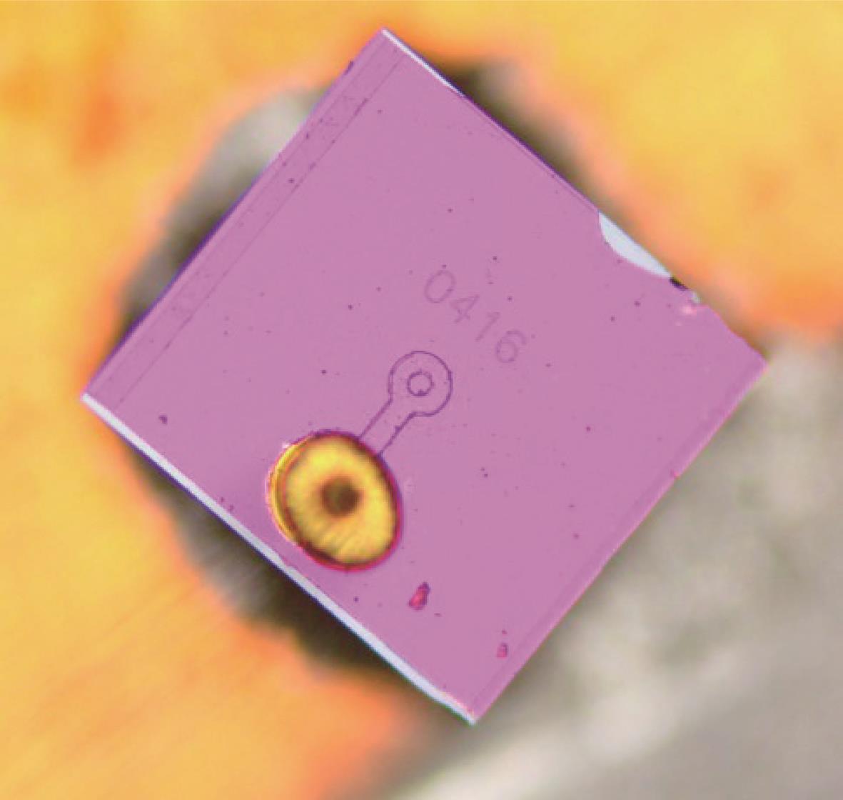
    Figure 1 shows top microscope image of a fabricated VCSEL. Wafers are grown on 2 inch Si-InP (100) substrates in a multiple-wafer metal organic chemical vapor deposition (MOCVD) reactor. The bottom DBR consists of over 45 pairs of InP and AlxGayIn(1-x-yAs lattice-matched to InP. The active region constitutes 6 strain compensated AlxGayIn(1-x-yAs/InP QWs. Above the active layers, a p++-AlxGayIn(1-x-yAs/n++-AlxGayIn(1-x-yAs tunnel junction is grown. Carbon was used as p-type dopant since carbon has low diffusivity compared with zinc [20]. The bandgap of AlxGayIn(1-x-yAs in the tunnel junction is higher than the photon energy at the lasing wavelength to avoid optical absorption. For the same purpose, the thin tunnel junction is designed at a node of the standing wave of the VCSELs. After the growth of the tunnel junction, a n-type InP layer was regrown. The whole wafer was patterned with photolithography and circular mesas were formed for blocking the current outside by proton implantation. Next, anode electrodes with Ti/Pt/Au were formed on the top side of n-type InP epitaxial layer as a contact structure to reduce the capacitance of devices. The top DBRs consist of amorphous-Si(α-Si) and SiO2 evaporated by e-beam evaporation. In addition, the wafer was pattered with photolithography and circular were formed by ICP to top pad contract window. Finally, cathode electrodes were formed on the bottom side of the substrate with Au/Ge/Ni.

    Top microscope image of fabricated VCSEL

    Figure 1.Top microscope image of fabricated VCSEL

    2 Results and discussion

    2.1 Current-light (I-L) characteristics

    Figure 2 shows the I-L characteristics of 1550 nm VCSELs with 12 µm diameter tunnel junction apertures at room temperature (about 20 ℃). The threshold current () is 20 mA. Output power () increases rapidly with driving current () above and the maximum output power was around 7 µW under CW 60 mA.

    I-L characteristics of fabricated VCSEL under CW operation at room temperature

    Figure 2.I-L characteristics of fabricated VCSEL under CW operation at room temperature

    is given by:

    Ith=Aajth=qVaηIτspnthqVaBηInt2exp2gth/g1

    is active material area. The threshold current density then follow as . is the elementary charge and is the current injection efficiency accounting for lateral leakage currents and carrier overflow over confining barriers. The spontaneous recombination lifetime depends on the carrier density. The term and have the meaning of a threshold carrier density and a transparency carrier density, respectively. The active volume with is active material thickness. is Boltzmann constant. The threshold gain is and is constant. From Eq. 1 , we can find that depends on ,, ect. In other words, when the numbers of quantum well in VCSEL devices is the same, the DBR reflectivity required is high to achieve low threshold current and high output power. As can be seen from Fig. 3, the cavity mode is located at 1 532 nm, the overall reflectance is 95%, and the reflectance is 94% at 1 532 nm. It can be concluded from the actual experimental value that the threshold current is 20 mA and the output power is 7 µW, indicating that the reflectance of DBR on both sides of the quantum well is low in the actual value, the transmittance of the cavity mode position is about 1%, resulting in the low output power of the device. Subsequently, the reflectivity of the upper and bottom DBR should be increased.

    Reflection spectra and the cavity mode of the VCSEL structure

    Figure 3.Reflection spectra and the cavity mode of the VCSEL structure

    is given by [21]:

    Pout=ηeωqI-Ith

    VI=V0+IRs

    where is differential quantum efficiency. is Planck constant, . is photon frequency. denotes the differential series resistance. The kink voltage is related to the separation of quasi-Fermi energies but can be approximated by .

    ηcI=PoutIV=ηeν/q(I-Ith)I(V0+IRs)

    Equation 4 shows that for >> the series resistance is responsible for the decrease of with increasing current. Efficiency is maximized at the laser current

    with . (5)

    From which the maximum conversion efficiency is obtained as

    ηmax=ηeνqV0ξ1+1+ξ2=ηeνqV0fcξ

    PmaxI0=ηeν/qIth1+ξ

    It becomes clear that obtaining maximum conversion efficiency is one of the most challenging topics increasing the factor of , namely increasing the production of threshold current and resistance[22]. On the other hand, differential quantum efficiency is defined as the ratio of mirror loss and mirror loss plus internal loss.

    ηe=τpτp,mαmαi+αm=11-αiLeff/lnRtRb

    where is proton lifetime, is proton lifetime including mirror loss. is mirror loss from emission through the top and bottom mirror. is internal loss. is effective cavity length. is top mirror reflectivity. is bottom mirror reflectivity. As shown Eqs. 2-8, the main reasons for output power are followed by: (1) The strongest increase occurs with the horizontal electron leakage. This leakage current from the MQW active region into devices. In order to confine current, we can improve that buried tunnel junction can be employed. (2) The heating from device leads to a reduction of the differential quantum efficiency. Heat sink TEC can be added to control device temperature. (3) During the epitaxial growth, the interface is not ideal in the experiment process. Four times lithography processes before sputtering SiO2/Si DBR are used. Any particle residue in the interface after the cleaning process or the reflectance coatings poor quality can lead to light absorption and loss. We should strictly control the processed or adjustment processes order.

    The typical I-V characteristics of devices are shown in Fig.4. From Eq.3, the kink voltage is related to the separation of quasi-Fermi energies but can be approximated by . The resistance for the 12-µm devices is around 25 Ω.As is shown in Fig.3, the temperature dependence of I-V characteristics of sample is measured under CW operation. This is because the current path is like structure of a half cavity. The voltage and series resistance decrease as increasing temperature from Fig. 4, which is in band gap narrowing and barrier height declining from heterojunction.

    I-V characteristics of fabricated VCSELs under CW operation at room temperature

    Figure 4.I-V characteristics of fabricated VCSELs under CW operation at room temperature

    2.2 Lasing spectra

    The emission wavelength of a VCSEL is controlled by the resonator rather than the spectral position of the gain peak. For perfect alignment with emission wavelength,we have peak gain . Figure 5 shows spectra under different injected current of 25, 40 and 60 mA. Single fundamental transverse mode operation was achieved for different current range. The wavelengths under different injected current are 1 551 nm, 1 552 nm and 1 554 nm under different injected current respectively. The wavelength shows that the center reflectivity spectrum of bottom DBR, gain and the center reflectivity spectrum of top DBR are matched with each other. The main reason of wavelength shift with different injected current is caused by Joule heat[23], which is mainly generated in the p-doped layers. Recombination heat is generated in the quantum wells, as well as negative Thomson heat which accounts for the capture and escape of quantum-well carriers (carrier escape requires energy and it removes heat from the lattice). Optical absorption heat is also strongest in the quantum wells due to absorption by holes. On the other hand, the cavity mode has red shift with the increase of temperature, which leads to lasing spectrum drift, mainly because the refractive index of AlxGayIn(1-x-yAs material increases with the steady rise, and finally leads to the overall reflectance red shift of the device. Since the refractive index of AlxGayIn(1-x-yAs material changes very little with the temperature, the spectral drift rate is also very small. The full width at half maximum(FWHM) of lasing spectrum is about 3 nm under 60 mA current injected.

    The lasing spectra of fabricate VCSEL

    Figure 5.The lasing spectra of fabricate VCSEL

    3 Conclusions

    In summary, the lasing operation of 1550 nm VCSELs has been demonstrated. The electrical properties of VCSEL were studied using I-V charactics and I-P charactics measurents. The threshold current was 20 mA and the maximum output power was around 7 µW under CW 60 mA. The wavelength of lasing spectra is 1 554 nm and the FWHM is 3 nm. We analyse the threshold current and output power from both theory and experiments. We believe that InP-based VCSELs can be strong candidates for low-cost and long-reach optical interconnects.

    References

    [1] V Iakovlev, G Suruceanu, A Caliman. High-performance single-mode VCSELs in the 1310-nm waveband. IEEE photonics technology letters, 17, 947-949(2005).

    [2] Koyama K, Advances and new functions of VCSEL photonics. Optical Review, 21, 893-904(2014).

    [3] C Chang-hasnain. Progress and prospects of long-wavelenght VCSELs. IEEE Communications Magazine, 41, S30-S34(2003).

    [5] E Kapon, A Sirbu. Power-efficient answer. Nature Photonics, 3, 27-29(2009).

    [6] Chepkoiwo Cherutoi. 310 nm and 1 550 nm transmission wavelengths. American Journal of Optics and Photonics, 5, 73-79(2017).

    [7] A Karthikeyan, P S Mallick. High-speed and low-power repeater for VLSI interconnects. Journal of Semiconductors, 38, 105006-1-105006-5(2017).

    [8] X Wang, J F Liu. Emerging technologies in Si active photonics. Journal of Semiconductors, 39, 061001-1-061001-29(2018).

    [9] N Nishiyama, C Caneau, B Hall. Long-wavelength vertical-cavity surface-emitting lasers on InP with lattice matched AlGaInAs-InP DBR grown by MOCVD. IEEE Journal of Selected Topics in Quantum Electronics, 11, 990-998(2005).

    [10] C J Chang-Hasnain. Tunable VCSEL. IEEE Journal of Selected Topics in Quantum Electronics, 6, 978-987(2000).

    [11] K Li, Y Rao, C Chase. Monolithic high-contrast metastructure for beam-shaping VCSELs. Optica, 5, 10-13(2018).

    [12] C Chase*a, Y Raoa, M Huanga. Tunable 1550 nm VCSELs using high contrast grating for next-generation networks. SPIE, 9008, 900807-1-900807-5(2014).

    [13] R Shau*a, M Ortsieferb, J Rosskopfb. Long-wavelength InP-based VCSELs with buried tunnel junctions: Properties and applications. SPIE, 5364, 1-15(2004).

    [14] M Muller, W Hofmann, T Grundl. 1550-nm High-Speed Short-Cavity VCSELs. IEEE Journal of Selected Topics in Quantum Electronics, 17, 1158-1166(2011).

    [15] K Zogal, T Gruendl, H A Dacani. 55-µm MEMS-tunable VCSEL(2011).

    [16] S Hu, X Y He, Y He. Impact of damping on high speed 850 nm VCSEL performance. Journal of Semiconductors, 39, 114006-1-114006-4(2018).

    [17] G Z Shi. Study of wavelength tunable vertical-cavity surface-emitting lasers(2013).

    [19] 19http://mp.weixin.qq.com/s/eOK1fpzgvXy5Gq-O_eUB0A (2017/03/02) http://mp.weixin.qq.com/s/eOK1fpzgvXy5Gq-O_eUB0A (2017/03/02

    [20] C Caneau, R Bhat, S Goswami. OMVPE grown GaInAs:C for HBTs. Journal of Electronics Materials, 25, 491-494(1996).

    [21] 21RhodesW T, et al., Fundamentals of fiber lasers and fiber amplifiers [M]. Berlin:Springer2013,1-235.

    [22] A Islam, S Islam. Designing a high speed 1 310 nm AlGaInAs/AlGaInAs VCSEL using MgO/Si top DBR and GaInAsP/InP bottom DBR. American Journal of Optics and Photonics, 2, 38-44(2014).

    [23] T Shih, Y C Chi, R N Wang. Efficient heat dissipation of uncooled 400-Gbps (16×25-Gbps) optical transceiver employing multimode VCSEL and PD arrays. Scientific Reports, 7, 1-10(2017).

    Li-Jie LIU, Yuan-Da WU, Yue WANG, Liang-Liang WANG, Jun-Ming An, You-Wen ZHAO. 1 550 nm VCSELs for long-reach optical interconnects[J]. Journal of Infrared and Millimeter Waves, 2020, 39(4): 397
    Download Citation