• Journal of Semiconductors
  • Vol. 45, Issue 3, 032501 (2024)
Nicolò Zagni1、*, Manuel Fregolent2、**, Andrea Del Fiol2, Davide Favero2, Francesco Bergamin2, Giovanni Verzellesi3、4, Carlo De Santi2, Gaudenzio Meneghesso2, Enrico Zanoni2, Christian Huber5, Matteo Meneghini2, and Paolo Pavan1
Author Affiliations
  • 1Department of Engineering “Enzo Ferrari”, University of Modena and Reggio Emilia, Modena 41125, Italy
  • 2Department of Information Engineering, University of Padova, Padova 35131, Italy
  • 3Department of Sciences and Methods for Engineering (DISMI), University of Modena and Reggio Emilia, Reggio Emilia 42122, Italy
  • 4EN & TECH Center, University of Modena and Reggio Emilia, Reggio Emilia 42122, Italy
  • 5Advanced Technologies and Micro Systems Department, Robert Bosch GmbH, Renningen 71272, Germany
  • show less
    DOI: 10.1088/1674-4926/45/3/032501 Cite this Article
    Nicolò Zagni, Manuel Fregolent, Andrea Del Fiol, Davide Favero, Francesco Bergamin, Giovanni Verzellesi, Carlo De Santi, Gaudenzio Meneghesso, Enrico Zanoni, Christian Huber, Matteo Meneghini, Paolo Pavan. Physical insights into trapping effects on vertical GaN-on-Si trench MOSFETs from TCAD[J]. Journal of Semiconductors, 2024, 45(3): 032501 Copy Citation Text show less
    (Color online) (a) Schematic 2-D view of the pseudo-vertical GaN-on-Si TMOS under study in this work. (b) TEM image of a FIB lamella taken from the gate trench.
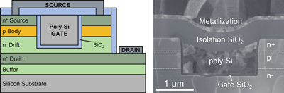
    Fig. 1. (Color online) (a) Schematic 2-D view of the pseudo-vertical GaN-on-Si TMOS under study in this work. (b) TEM image of a FIB lamella taken from the gate trench.
    HRTEM image at 820 Kx magnification of the gate interface in the channel region on the etched sidewall for device B.
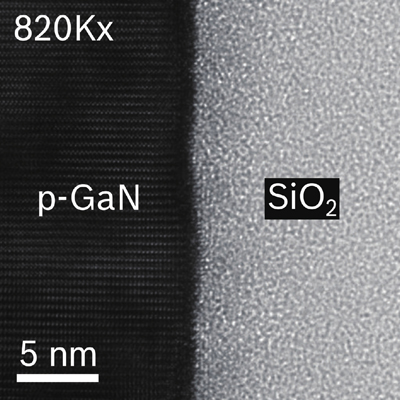
    Fig. 2. HRTEM image at 820 Kx magnification of the gate interface in the channel region on the etched sidewall for device B.
    (Color online) Experimentally measured ID−VGS of device A (a) and B (b). Continuous lines with squares (dashed lines with circles) are the forward and backward sweeps, respectively.
    Fig. 3. (Color online) Experimentally measured IDVGS of device A (a) and B (b). Continuous lines with squares (dashed lines with circles) are the forward and backward sweeps, respectively.
    (Color online) VT time evolution during (a) stress and (b) recovery experiments on device B. Different stress voltages (VGS,STR) were applied (see legend), whereas the recovery voltage (VGS,REC) was always 0 V.
    Fig. 4. (Color online) VT time evolution during (a) stress and (b) recovery experiments on device B. Different stress voltages (VGS,STR) were applied (see legend), whereas the recovery voltage (VGS,REC) was always 0 V.
    (Color online) VT time evolution during (a) stress (VGS,STR = 30 V) and (b) recovery (VGS,REC = 0 V) experiments on device A and different temperatures (see legend). No clear dependence of VT shift on temperature was found.
    Fig. 5. (Color online) VT time evolution during (a) stress (VGS,STR = 30 V) and (b) recovery (VGS,REC = 0 V) experiments on device A and different temperatures (see legend). No clear dependence of VT shift on temperature was found.
    (Color online) (a) Interface and (b) border trap densities vs trap energy (ET) referred to the conduction band edge of GaN (EC) employed in the simulations of device A (for device B, all parameters were the same except for the concentrations, see Table 1). ECNL in (a) indicates the assumed charge neutrality level that discriminates between acceptor-like and donor-like interface traps[22]. Border traps are only acceptor states.
    Fig. 6. (Color online) (a) Interface and (b) border trap densities vs trap energy (ET) referred to the conduction band edge of GaN (EC) employed in the simulations of device A (for device B, all parameters were the same except for the concentrations, see Table 1). ECNL in (a) indicates the assumed charge neutrality level that discriminates between acceptor-like and donor-like interface traps[22]. Border traps are only acceptor states.
    (Color online) Simulated ID−VGS of device A (a) and B (b). Continuous (dashed) lines are the forward and backward sweeps, respectively.
    Fig. 7. (Color online) Simulated IDVGS of device A (a) and B (b). Continuous (dashed) lines are the forward and backward sweeps, respectively.
    (Color online) (a) Simulated band diagram (device B) plotted along the lateral dimension perpendicular to the vertical current flow for different VGS (see legend). (b) Corresponding trapped charge in border traps (nBT) in the gate oxide (SiO2) and free electron density (n) in the channel (GaN).
    Fig. 8. (Color online) (a) Simulated band diagram (device B) plotted along the lateral dimension perpendicular to the vertical current flow for different VGS (see legend). (b) Corresponding trapped charge in border traps (nBT) in the gate oxide (SiO2) and free electron density (n) in the channel (GaN).
    (Color online) (a) Simulated band diagram (device B) plotted along the lateral dimension perpendicular to the vertical current flow for different VGS (see legend). (b) Corresponding trapped charge in border traps (nBT) in the gate oxide (SiO2) and free electron density (n) in the channel (GaN).
    Fig. 9. (Color online) (a) Simulated band diagram (device B) plotted along the lateral dimension perpendicular to the vertical current flow for different VGS (see legend). (b) Corresponding trapped charge in border traps (nBT) in the gate oxide (SiO2) and free electron density (n) in the channel (GaN).
    (Color online) Hysteresis in the ID−VGS (see text for definition) of device A and B. Both experimental data and simulation results are shown. Dashed lines are linear fitting of data points. The ≈75% hysteresis reduction at VGS,max = 40 V of device B compared to A is reproduced by simulations by reducing oxide trap concentration by the same amount.
    Fig. 10. (Color online) Hysteresis in the IDVGS (see text for definition) of device A and B. Both experimental data and simulation results are shown. Dashed lines are linear fitting of data points. The ≈75% hysteresis reduction at VGS,max = 40 V of device B compared to A is reproduced by simulations by reducing oxide trap concentration by the same amount.
    (Color online) Sensitivity of H to border trap density (DBT) with the simulation setup calibrated on device B. The experimental data points at VGS,max = 40 V are shown for reference.
    Fig. 11. (Color online) Sensitivity of H to border trap density (DBT) with the simulation setup calibrated on device B. The experimental data points at VGS,max = 40 V are shown for reference.
    (Color online) Sensitivity of SS (obtained on the upward sweep) to interface trap density (DIT) with the simulation setup calibrated on device B. The experimental data points at VGS,max = 40 V are shown for reference. The asymptotic theoretical limit (i.e., for a trap-free interface determined only by the depletion capacitance, CD, and oxide capacitance, Cox) is also indicated.
    Fig. 12. (Color online) Sensitivity of SS (obtained on the upward sweep) to interface trap density (DIT) with the simulation setup calibrated on device B. The experimental data points at VGS,max = 40 V are shown for reference. The asymptotic theoretical limit (i.e., for a trap-free interface determined only by the depletion capacitance, CD, and oxide capacitance, Cox) is also indicated.
    Label*Areal density (DIT, cm−2∙eV−1)Volume density (DBT, cm−3∙eV−1)Energy mean** (EM, eV)Energy spread(ES, eV)
    *A stands for acceptors, D for donors. **With respect to GaN conduction band edge (EC).
    IT, A1 × 1013/5 × 1012//00.2
    IT, D2 × 1012/1 × 1012//0.91.6
    BT, A//4 × 1019/1 × 101902
    Table 1. Trap-related simulation parameters (Device A/Device B).
    Nicolò Zagni, Manuel Fregolent, Andrea Del Fiol, Davide Favero, Francesco Bergamin, Giovanni Verzellesi, Carlo De Santi, Gaudenzio Meneghesso, Enrico Zanoni, Christian Huber, Matteo Meneghini, Paolo Pavan. Physical insights into trapping effects on vertical GaN-on-Si trench MOSFETs from TCAD[J]. Journal of Semiconductors, 2024, 45(3): 032501
    Download Citation