Nicolò Zagni1、*, Manuel Fregolent2、**, Andrea Del Fiol2, Davide Favero2, Francesco Bergamin2, Giovanni Verzellesi3、4, Carlo De Santi2, Gaudenzio Meneghesso2, Enrico Zanoni2, Christian Huber5, Matteo Meneghini2, and Paolo Pavan1
Nicolò Zagni, Manuel Fregolent, Andrea Del Fiol, Davide Favero, Francesco Bergamin, Giovanni Verzellesi, Carlo De Santi, Gaudenzio Meneghesso, Enrico Zanoni, Christian Huber, Matteo Meneghini, Paolo Pavan. Physical insights into trapping effects on vertical GaN-on-Si trench MOSFETs from TCAD[J]. Journal of Semiconductors, 2024, 45(3): 032501
Copy Citation Text
Vertical GaN power MOSFET is a novel technology that offers great potential for power switching applications. Being still in an early development phase, vertical GaN devices are yet to be fully optimized and require careful studies to foster their development. In this work, we report on the physical insights into device performance improvements obtained during the development of vertical GaN-on-Si trench MOSFETs (TMOS’s) provided by TCAD simulations, enhancing the dependability of the adopted process optimization approaches. Specifically, two different TMOS devices are compared in terms of transfer-curve hysteresis (H) and subthreshold slope (SS), showing a ≈ 75% H reduction along with a ≈ 30% SS decrease. Simulations allow attributing the achieved improvements to a decrease in the border and interface traps, respectively. A sensitivity analysis is also carried out, allowing to quantify the additional trap density reduction required to minimize both figures of merit.
Lateral gallium-nitride (GaN) field-effect transistors are currently employed as switches for efficient power conversion. While lateral GaN high electron mobility transistors (HEMTs) are already commercially available, vertical counterparts are still in a relatively early development phase, and intensive research is undergoing to harness their advantages over the lateral devices in high power applications[1, 2]. These advantages stem from the fact that in vertical transistors the drift region develops through the device depth instead of length. This design allows an increase in the maximum blocking voltage without extending the device laterally and allows for the peak electric field to be far from the device surface, enhancing both stability and reliability[2, 3]. Consequently, vertical devices operating safely in the kV range can be designed with a relatively small chip area and are naturally immune from common drawbacks that vex lateral devices operation (e.g., current-collapse, dynamic Ron, etc.)[3−7]. Furthermore, reliable and unclamped inductive switching in converter circuits employing vertical GaN devices can be achieved thanks to their avalanche capability[8−10]. However, vertical GaN devices are yet to be fully optimized and suffer from stability and reliability issues of their own[11], particularly regarding the gate oxide and its interface with GaN[2, 11−13].
In this work, we investigated the influence of gate oxide optimization on the transfer characteristics hysteresis (H) and subthreshold-slope (SS) of two pseudo-vertical GaN-on-Si trench MOSFETs (TMOS’s), labelled device A and B, with different gate stack deposition technique. Experimental characterization was carried out to quantify the hysteresis and its dependence on the maximum gate−source voltage applied, whereas TCAD simulations were adopted to gain insight into the observed H and SS reduction obtained with device B with respect to device A. Our analysis allows to entirely attribute the presence of the hysteresis to electron trapping into border traps, i.e., to trap states located in the gate oxide at a tunneling range from the oxide/semiconductor interface, and the observed H improvement from device A to device B to a 4 × reduction in the border-trap density. SS is instead mainly governed by interface traps and its improvement can be ascribed to a 2 × decrease in their density. Moreover, the mobility improvement between the two devices can be attributed to increased SiO2/GaN interface quality, which reduces the amount of interface traps.
Devices and experimental results
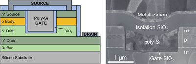
Devices under test (DUT’s) in this work are pseudo-vertical GaN trench MOSFETs (TMOS’s) on 150 mm GaN-on-Si wafers. The MOS gate stack was based on an LPCVD SiO2 gate dielectric with polysilicon gate electrode which has previously been shown to be suitable for GaN planar MOSFETs[14, 15]. The schematic 2-D device structure is shown in Fig. 1. The epitaxial GaN stack from bottom to top consists of a strain-relief buffer layer and a n+ drain layer (1 µm) to achieve ohmic contact with the drain metal. The drain contact is deposited on the surface laterally with respect to the device active mesa region which consists of a n− drift region (1 µm), a p body channel region (0.5 µm), and a n+ source layer (0.3 µm). The nominal magnesium concentration in the p body layer is 1019 cm−3. It should be noted that the thickness of n− drift region is too low to block considerable voltages. Indeed, its thickness was chosen such that its resistance contribution is minor compared to the channel resistance. The gate trench was formed by chlorine plasma etching followed by wet treatment in TMAH to reduce crystal damage induced by the dry etch process and selectively prepare the m-plane of the GaN crystal.
Figure 1.(Color online) (a) Schematic 2-D view of the pseudo-vertical GaN-on-Si TMOS under study in this work. (b) TEM image of a FIB lamella taken from the gate trench.
The deposition of the 70-nm silicon dioxide (SiO2) single-layer gate dielectric differed in the two devices (A and B) considered in this work. For device A, gate oxide was deposited by low-pressure chemical vapor deposition at 785 °C with a post-deposition anneal at 800 °C, whereas for device B, SiO2 deposition was carried out at 880 °C with a post-deposition anneal at 900 °C. It was previously found that such an annealing treatment improves the field effect mobility in the channel of lateral channel MOSFETs[15].
Fig. 1(b) shows a TEM image of the gate trench for device B. It can be seen that fabrication resulted in straight trenched sidewalls with a smooth interface between semiconductor and dielectric perpendicular to the c-planes, as also shown by the HRTEM image at 820 Kx magnification in Fig. 2. Both device A and B were characterized with Keysight 5260 source measurement units (SMU's) by performing a back-and-forth gate-to-source voltage (VGS) sweep in DC regime while keeping the drain-to-source voltage (VDS) fixed at 1 V and recording the drain current (ID). A set of ID−VGS transfer characteristics were acquired by increasing the maximum applied voltage (VGS,max) from 5 to 40 V; the minimum applied VGS was always –5 V. The sweep rate was 1 V/s, and the bias step was 100 mV. Note that 40 V is the maximum allowed bias to avoid excessive gate leakage, while typically maximum bias during device operation is ≤20 V.
Figure 2.HRTEM image at 820 Kx magnification of the gate interface in the channel region on the etched sidewall for device B.
To restore the state of the device and avoid trapped charge accumulation, after each sweep the DUT’s were exposed to 365 nm (3.4 eV) ultraviolet (UV) illumination for a few minutes. Experimental data are collected in Fig. 3, showing the set of ID−VGS curves for device A (a) and B (b) for different VGS,max. Saturation current (ID,SS) at VDS = 5 V and VGS = 20 V is 0.12 mA/mm and 0.2 A/mm for device A and B, respectively. The main factors limiting ID,SS are the mobility degradation due to electron conduction near the semiconductor/oxide interface and the Fermi level pinning due to charged acceptor interface and border traps.
Figure 3.(Color online) Experimentally measured ID−VGS of device A (a) and B (b). Continuous lines with squares (dashed lines with circles) are the forward and backward sweeps, respectively.
The almost overlapping threshold voltage (VT) of the forward ID−VGS curves for both devices indicates that the 3.4 eV UV light is effective in restoring the state of the device. On the other hand, at room temperature it was found that 100-s recovery phase at VGS = 0 V after 100-s stress at VGS = 40 V led to a residual ≈2 V positive VT shift, i.e., full recovery was not achieved, see Fig. 4.
Figure 4.(Color online) VT time evolution during (a) stress and (b) recovery experiments on device B. Different stress voltages (VGS,STR) were applied (see legend), whereas the recovery voltage (VGS,REC) was always 0 V.
For both devices, we observed a VT shift between the forward and backward sweep, indicating that slow traps get filled with electrons during the forward sweep and are not thermally emitted during the backward sweep. The VT difference between the backward and forward sweep is commonly referred to as hysteresis. Note that VT is taken at VGS for which ID = 1 μA/mm. Because the amount of trapped charge increases with increasing VGS,max, hysteresis is also proportional to VGS,max[16]. As can be noted by comparing Figs. 3(a) and 3(b), device B hysteresis is remarkedly lower than that of device A. This behavior is further investigated by means of numerical simulations in Section 3.
In general, both electron trapping and detrapping are dynamic processes that determine a positive/negative VT drift, respectively, and as such these VT drifts are proportional to the duration of bias application. Non-zero hysteresis can thus be interpreted as the net result of electron trapping followed by an electron release that is not fully completed in the time window of the applied VGS range.
Fig. 4 better clarifies this point, showing the VT drift during stress/recovery experiments carried out for several time decades (from 10 μs to 100 s) at different stress voltages (VGS,STR) and at a fixed 0 V recovery bias (VGS,REC) on device B. During stress and recovery cycles, stress (recovery) bias was periodically turned off to allow the measurement of the ID−VGS curve to probe VT, by sweeping VGS from 0 to 30 V in 10 μs with VDS = 1 V. In this case, due to insufficient resolution of the experimental setup at low currents, VT was taken at ID = 1 mA/mm. The non-saturating behavior of VT shift with both stress and recovery time in Fig. 4 is in agreement with previous studies of PBTI on GaN-based planar devices[17−19].
Looking, for instance, at the case VGS,STR = 40 V in Fig. 4, the net VT drift (taken as the difference between the value at the beginning of the stress cycle and that at the end of the recovery one) is about 2 V, which correlates nicely with hysteresis at VGS,max = 40 V as shown in Fig. 3 (and Fig. 7). This result suggests that non-zero hysteresis can be interpreted as the net result of the dynamic processes of electron trapping and incomplete recovery (from trapping) in the time window of the applied VGS sweep.
Furthermore, VT drift during stress at VGS,STR = 30 V was characterized at different temperatures to better understand the physical mechanism at the origin of hysteresis. Fig. 5 shows the results of this characterization on device A, and it can be observed that VT drift during stress is not influenced by temperature, supporting the hypothesis of tunneling as the underlying mechanism. A more detailed discussion of the VT shift during stress and recovery experiments is provided in Ref. [20].
Figure 5.(Color online) VT time evolution during (a) stress (VGS,STR = 30 V) and (b) recovery (VGS,REC = 0 V) experiments on device A and different temperatures (see legend). No clear dependence of VT shift on temperature was found.
Two-dimensional numerical device simulations were performed with the Synopsys TCAD tool SDevice[21] aimed at obtaining insights on the improvement in the stability of ID−VGS curves of the two devices discussed in Section 2. Particularly, we investigated the impact of border and interface traps on hysteresis and subthreshold slope reduction. Charging and discharging of interface traps are accounted for by means of a fully dynamic SRH model (no quasi-static approximation), that is self-consistently coupled to the drift-diffusion equations. Additionally, border traps are placed into SiO2 gate oxide region and are allowed to exchange electrons with the GaN surface through the nonlocal “tunneling into traps” model included in the simulator[21]. A constant mobility model, which is only dependent on temperature, was adopted for simplicity. Hence, technological development in terms of mobility improvement is reproduced in the simulations by setting the channel mobility value (μch) in the body layer (i.e., where the inversion channel forms) for the two devices to the respective field-effect mobility extracted from the measurements.
The energy distributions and concentration of interface (IT) and border traps (BT), as well as channel mobility, were firstly calibrated to obtain a best fitting with the experimentally measured hysteresis on device A. Box-like distributions for trap distributions were adopted for a more straightforward parametrization. The trap parameters are summarized in Table 1.
Label*
Areal density (DIT, cm−2∙eV−1)
Volume density (DBT, cm−3∙eV−1)
Energy mean** (EM, eV)
Energy spread(ES, eV)
*A stands for acceptors, D for donors. **With respect to GaN conduction band edge (EC).
The box-like distribution has the following form[21]:
where DT is either DBT or DIT (see Table 1). EM and ES are defined in Table 1. We assume that the donor interface traps have a large energy distribution across the upper portion of GaN energy gap and that the acceptor interface traps are narrowly distributed near the conduction band edge (EC), which corresponds to assume that the charge neutrality level[23] is located 0.1 eV below EC. Interface and border traps distribution employed in the simulations are shown in Fig. 6. The interface trap distribution was modeled starting from the distribution experimentally validated for other material systems (e.g., Si−SiO2 interface[24], Al2O3−InGaAs interface[16]) and conventionally assumed for oxide/semiconductor interfaces[22]. Border trap distribution parameters were set in order to reproduce experimentally measured hysteresis.
Figure 6.(Color online) (a) Interface and (b) border trap densities vs trap energy (ET) referred to the conduction band edge of GaN (EC) employed in the simulations of device A (for device B, all parameters were the same except for the concentrations, see Table 1). ECNL in (a) indicates the assumed charge neutrality level that discriminates between acceptor-like and donor-like interface traps[22]. Border traps are only acceptor states.
The channel mobility (μch) was set to 3 cm2/(V∙s), corresponding to the field-effect mobility extracted from the measurements. The results of the simulations of device A in terms of ID−VGS curves for different VGS,max (VDS = 1 V) are shown in Fig. 7(a). Good agreement is obtained between experiments and simulations, compare Fig. 7(a) and Fig. 3(a). Hysteresis is physically induced by channel electron tunneling into the border traps during the upward VGS sweep and only partial electron release during the downward one, resulting in a right-shifted threshold voltage.
Figure 7.(Color online) Simulated ID−VGS of device A (a) and B (b). Continuous (dashed) lines are the forward and backward sweeps, respectively.
By properly reducing the IT and BT concentrations, as well as increasing channel mobility, without adjusting any other parameter, we calibrated the simulation results on device B as well, as shown by the ID−VGS curves in Fig. 7(b). The trap parameters are again reported in Table 1. μch in this case was set to 17 cm2/(V∙s), corresponding to the field-effect mobility extracted from the measurements.
The physical mechanism of hysteresis can be better understood with the aid of Fig. 8(a), showing the simulated band diagram across the channel (i.e., plotted along the lateral dimension perpendicular to the vertical current flow) for different VGS (see legend). Additionally, Fig. 8(b) shows the concentration of trapped charge in the oxide (nBT) and free electron density (n) in the channel corresponding to the same biases. As VGS increases, so does n in the channel as the Fermi level moves above the conduction band edge (i.e., inversion occurs). The raise in Fermi level position (with respect to EC) increases the probability for electron tunneling from the channel to the traps in the gate oxide (border traps). This consequently increases nBT in the same region, as shown in Fig. 8(b).
Figure 8.(Color online) (a) Simulated band diagram (device B) plotted along the lateral dimension perpendicular to the vertical current flow for different VGS (see legend). (b) Corresponding trapped charge in border traps (nBT) in the gate oxide (SiO2) and free electron density (n) in the channel (GaN).
Fig. 9 shows the same quantities as Fig. 8 but taken on the forward and backward curves at the same bias of VGS = 5 V. The larger nBT on the backward curve compared to the forward one causes a smaller n in the channel, see Fig. 9(b), leading to higher VT (and thus, hysteresis). This is consistent with the band diagrams shown in Fig. 9(a), as the band bending corresponding to VGS = 5 V on the backward curve is less than that on the forward one, meaning that inversion is weaker in the former than in the latter case, thus explaining the reduced n.
Figure 9.(Color online) (a) Simulated band diagram (device B) plotted along the lateral dimension perpendicular to the vertical current flow for different VGS (see legend). (b) Corresponding trapped charge in border traps (nBT) in the gate oxide (SiO2) and free electron density (n) in the channel (GaN).
The agreement between the simulations and experimental data in terms of hysteresis is further confirmed by Fig. 10, that shows how the calibrated setups are able to capture the linear dependence of hysteresis on VGS,max for both TMOS devices. Remarkably, the hysteresis reduction observed between the two devices of ≈75% at VGS,max = 40 V is captured by the simulations when reducing the BT density from 4 × 10¹⁹ eV–1∙cm–3 to 1 × 10¹⁹ eV–1∙cm–3. As stated earlier, typical gate bias during actual device operation is 20 V so that H in practice is <1 V for device B.
Figure 10.(Color online) Hysteresis in the ID−VGS (see text for definition) of device A and B. Both experimental data and simulation results are shown. Dashed lines are linear fitting of data points. The ≈75% hysteresis reduction at VGS,max = 40 V of device B compared to A is reproduced by simulations by reducing oxide trap concentration by the same amount.
IT concentration has little role on the hysteresis, due to the short emission time constants and fast charge (during upward VGS sweep) and discharge (backward VGS sweep)[16]; however, the IT density reduction favorably impacts SS, besides correlating with the mobility improvement as a result of the interface quality improvement[25].
By extending the BT and IT density range, it is possible to extrapolate the corresponding H and SS values, particularly to estimate the amount of trap density reduction required to minimize both H and SS. Fig. 11 shows the results of this analysis for the hysteresis vs BT density curve (with all other parameters of the setup calibrated on the experimental data of device B). This analysis reveals a strong dependence of hysteresis on BT density in the 5 × 10¹⁸ − 5 × 10¹⁹ eV–1∙cm–3 range: the higher the trap density, the higher the concentration of trapped electrons that cause the VT shift between forward and backward sweeps. Further reducing BT density below 1019 eV–1∙cm–3 leads to negligible hysteresis.
Figure 11.(Color online) Sensitivity of H to border trap density (DBT) with the simulation setup calibrated on device B. The experimental data points at VGS,max = 40 V are shown for reference.
Fig. 12 illustrates the dependence of SS on the interface trap density. As can be seen, the ≈30% SS reduction obtained by device B compared to device A is explained by TCAD simulations as a result of DIT reduction.
Figure 12.(Color online) Sensitivity of SS (obtained on the upward sweep) to interface trap density (DIT) with the simulation setup calibrated on device B. The experimental data points at VGS,max = 40 V are shown for reference. The asymptotic theoretical limit (i.e., for a trap-free interface determined only by the depletion capacitance, CD, and oxide capacitance, Cox) is also indicated.
We presented electrical characterization data and simulation results on two different pseudo-vertical GaN-on-Si trench MOSFETs. The higher temperature gate oxide deposition technique used in device B compared to device A led to a reduced transfer curve hysteresis and subthreshold slope, as well as increased channel mobility. Calibrated simulation decks on both devices allowed us to investigate in detail the cause for hysteresis, which can be attributed to oxide traps near the interface with the semiconductor (border traps). The subthreshold slope is instead mainly governed by the density of the interface traps. The improvements in hysteresis and subthreshold slope achieved by device B can therefore be attributed to a consistent decrease in the density of border and interface traps, respectively. The sensitivity analysis carried out by means of TCAD simulations in terms of hysteresis (subthreshold slope) vs border trap (interface trap) density, allows quantifying the additional trap density reduction required to minimize both figures of merit.
Nicolò Zagni, Manuel Fregolent, Andrea Del Fiol, Davide Favero, Francesco Bergamin, Giovanni Verzellesi, Carlo De Santi, Gaudenzio Meneghesso, Enrico Zanoni, Christian Huber, Matteo Meneghini, Paolo Pavan. Physical insights into trapping effects on vertical GaN-on-Si trench MOSFETs from TCAD[J]. Journal of Semiconductors, 2024, 45(3): 032501