• Journal of Semiconductors
  • Vol. 40, Issue 4, 042102 (2019)
Ruyue Cao1、2, Hui-Xiong Deng1、2, Jun-Wei Luo1、2、3, and Su-Huai Wei4
Author Affiliations
  • 1State Key Laboratory of Superlattices and Microstructures, Institute of Semiconductors, Chinese Academy of Sciences, Beijing 100083, China
  • 2University of Chinese Academy of Sciences, Beijing 100049, China
  • 3Synergetic Innovation Center of Quantum Information and Quantum Physics, University of Science and Technology of China, Hefei 230026, China
  • 4Beijing Computational Science Research Center, Beijing 100193, China
  • show less
    DOI: 10.1088/1674-4926/40/4/042102 Cite this Article
    Ruyue Cao, Hui-Xiong Deng, Jun-Wei Luo, Su-Huai Wei. Origin of the anomalous trends in band alignment of GaX/ZnGeX2 (X = N, P, As, Sb) heterojunctions[J]. Journal of Semiconductors, 2019, 40(4): 042102 Copy Citation Text show less
    (Color online) The crystal structure of superlattice GaX/ZnGeX2 (X = N, P, As, Sb). The Ga, Zn, Ge and X atoms are in light green, purple, gray and blue, respectively.
    Fig. 1. (Color online) The crystal structure of superlattice GaX/ZnGeX2 (X = N, P, As, Sb). The Ga, Zn, Ge and X atoms are in light green, purple, gray and blue, respectively.
    Band alignments of (a) GaN/ZnGeN2, (b) GaP/ZnGeP2, (c) GaAs/ZnGeAs2, (d) GaSb/ZnGeSb2 heterojunctions.
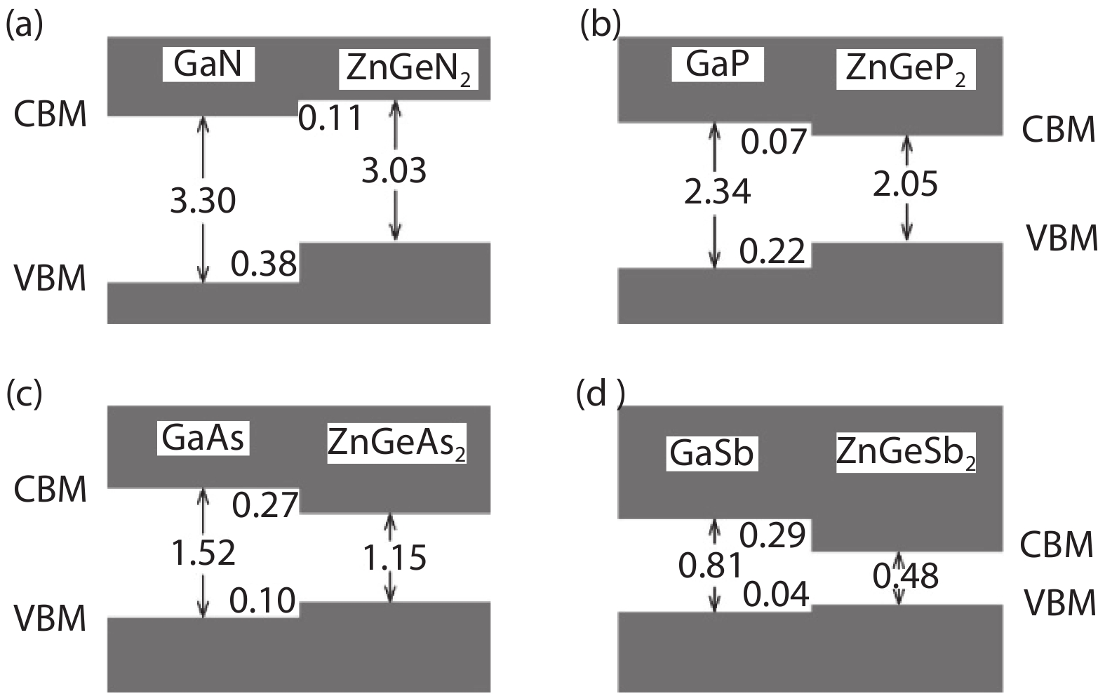
    Fig. 2. Band alignments of (a) GaN/ZnGeN2, (b) GaP/ZnGeP2, (c) GaAs/ZnGeAs2, (d) GaSb/ZnGeSb2 heterojunctions.
    (Color online) Band edge atomic orbital wavefunctions cubic GaAs and ZnGeAs2.
    Fig. 3. (Color online) Band edge atomic orbital wavefunctions cubic GaAs and ZnGeAs2.
    Contour plot of electron charge density of VBM and CBM states in () plane for GaX and corresponding plane in ZnGeX2 (X = N, P, As, Sb).
    Fig. 4. Contour plot of electron charge density of VBM and CBM states in ( ) plane for GaX and corresponding plane in ZnGeX2 (X = N, P, As, Sb).
    CrystalLattice constant (Å) HSE (Exp.)Bond length (Å) HSE (Exp.)Band gap (eV) HSE (Exp.)
    GaNa = b = c = 4.512 (4.50) 1.954 (1.949)3.12 (3.30[20])
    GaPa = b = c = 5.483 (5.45) 2.374 (2.360)2.32 (2.34[21])
    GaAsa = b = c = 5.695 (5.65) 2.466 (2.448)1.35 (1.52[20])
    GaSba = b = c = 6.154 (6.10) 2.665 (2.640)0.79 (0.81[20])
    ZnGeN2a = b = 4.572, c = 8.776 (Ge–N) 1.871, (Zn–N) 2.0433.03
    ZnGeP2a = b = 5.473 (5.46), c = 10.749 (10.76) (Ge–P) 2.334 (2.309), (Zn–P) 2.378 (2.398)2.02 (2.05[22])
    ZnGeAs2a = b = 5.711 (5.67), c = 11.226 (11.15) (Ge–As) 2.446 (2.396), (Zn–As) 2.472 (2.488)1.07 (1.15[23])
    ZnGeSb2a = b = 6.156, c = 12.193 (Ge–Sb) 2.664, (Zn–Sb) 2.6500.48
    Table 1. Calculated lattice constants, bond lengths and band gaps of GaX and ZnGeX2 (X = N, P, As, Sb) compounds using HSE functional compared with experimental values.
    OrbitNPAsSbZnGaGe
    n s −18.49−14.09−14.77−13.16−6.31−9.25−12.03
    n p −7.32−5.68−5.42−5.08−1.31−2.82−4.13
    (n − 1) d −40.60−33.32−10.49−19.18−29.57
    Table 2. Atomic energy levels (eV) of valence states of elements studied in this paper.
    Ruyue Cao, Hui-Xiong Deng, Jun-Wei Luo, Su-Huai Wei. Origin of the anomalous trends in band alignment of GaX/ZnGeX2 (X = N, P, As, Sb) heterojunctions[J]. Journal of Semiconductors, 2019, 40(4): 042102
    Download Citation