• Journal of Semiconductors
  • Vol. 40, Issue 1, 011802 (2019)
Hang Dong1、2, Huiwen Xue1、2, Qiming He1、2, Yuan Qin1、2, Guangzhong Jian1、2, Shibing Long1、2、3, and Ming Liu1、2
Author Affiliations
  • 1Key Laboratory of Microelectronic Devices & Integration Technology, Institute of Microelectronics of Chinese Academy of Sciences, Beijing 100029, China
  • 2University of Chinese Academy of Sciences, Beijing 100049, China
  • 3School of Microelectronics, University of Science and Technology of China, Hefei 230026, China
  • show less
    DOI: 10.1088/1674-4926/40/1/011802 Cite this Article
    Hang Dong, Huiwen Xue, Qiming He, Yuan Qin, Guangzhong Jian, Shibing Long, Ming Liu. Progress of power field effect transistor based on ultra-wide bandgap Ga2O3 semiconductor material[J]. Journal of Semiconductors, 2019, 40(1): 011802 Copy Citation Text show less
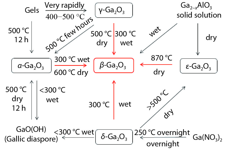
    (Color online) Transformation relationships among Ga2O3 in different crystalline phases and their hydrates[21].
    Fig. 1. (Color online) Transformation relationships among Ga2O3 in different crystalline phases and their hydrates[21].
    (Color online) Crystal structure of β-Ga2O3[32].
    Fig. 2. (Color online) Crystal structure of β-Ga2O3[32].
    (Color online) The development of β-Ga2O3 transistor in recent years.
    Fig. 3. (Color online) The development of β-Ga2O3 transistor in recent years.
    (Color online) Schematic cross-section of β-Ga2O3 (a) MESFET[12] and (b) MOSFET[11].
    Fig. 4. (Color online) Schematic cross-section of β-Ga2O3 (a) MESFET[12] and (b) MOSFET[11].
    (Color online) (a) Schematic cross-section, (b) the off-state drain/gate leakage and breakdown curves, (c) temperature-dependent transfer characteristics at Vds = 30 V, and (d) DC and pulsed output curves of the β-Ga2O3 FP-MOSFET[16].
    Fig. 5. (Color online) (a) Schematic cross-section, (b) the off-state drain/gate leakage and breakdown curves, (c) temperature-dependent transfer characteristics at Vds = 30 V, and (d) DC and pulsed output curves of the β-Ga2O3 FP-MOSFET[16].
    Top–down SEM image of the two-finger MOSFET on (100) β-Ga2O3[55].
    Fig. 6. Top–down SEM image of the two-finger MOSFET on (100) β-Ga2O3[55].
    (Color online) (a) SEM false-colored cross-section view of recessed-gate MOSFETs and HR-TEM of (b) its sidewall and (c) bottom facets of the gate-recess contact, (d) its gate-source and drain-source breakdown curves of both source-drain distances[15].
    Fig. 7. (Color online) (a) SEM false-colored cross-section view of recessed-gate MOSFETs and HR-TEM of (b) its sidewall and (c) bottom facets of the gate-recess contact, (d) its gate-source and drain-source breakdown curves of both source-drain distances[15].
    (Color online) (a) Schematic cross-section and SEM image, and (b) three-terminal off-state breakdown curves of vertical β-Ga2O3 Fin-MISFET[14].
    Fig. 8. (Color online) (a) Schematic cross-section and SEM image, and (b) three-terminal off-state breakdown curves of vertical β-Ga2O3 Fin-MISFET[14].
    (Color online) (a) Cross section schematic, (b) focused ion beam (FIB) cross sectional image, and (c) extrinsic small signal RF gain performance of RF β-Ga2O3 MOSFET[59].
    Fig. 9. (Color online) (a) Cross section schematic, (b) focused ion beam (FIB) cross sectional image, and (c) extrinsic small signal RF gain performance of RF β-Ga2O3 MOSFET[59].
    (Color online) (a) Schematic and (b) density-dependent field effect mobility of Silicon delta-doped β-Ga2O3 MESFET.
    Fig. 10. (Color online) (a) Schematic and (b) density-dependent field effect mobility of Silicon delta-doped β-Ga2O3 MESFET.
    (Color online) Depletion/enhancement-mode β-Ga2O3 on insulator (GOOI) FETs[17].
    Fig. 11. (Color online) Depletion/enhancement-mode β-Ga2O3 on insulator (GOOI) FETs[17].
    Semiconductor materialSiGaN4H-SiCβ-Ga2O3
    Bandgap Eg (eV) 1.13.43.34.7–4.9
    Electron mobility μ (cm2·V−1·s−1) 140012001000300
    Breakdown electric field Eb (MV/cm) 0.33.32.58
    Baliga’s FOM (εμEb3) 18703403444
    Thermal conductivity λ (W·cm−1·K−1) 1.52.12.70.11
    Table 1. Comparison of the physical properties of Si, GaN, SiC and β-Ga2O3 semiconductor[6].
    Device typeSubstrateorientationGate dielectricsVbr (V) Jmax (mA/mm) On/off ratiogm (mS/mm) Reference
    D-MESFET(010) β-Ga2O32501041.4[12]
    D-MOSFET(010) β-Ga2O3Al2O3370391010[11]
    E-Fin FET(100) β-Ga2O3Al2O3600-105[15]
    Two-finger D-MOSFET(100) β-Ga2O3Al2O3230601071.1[55]
    Field plate D-MOSFET(010) β-Ga2O3Al2O3750781093.4[16]
    Recessed-gate D-MOSFET(100) β-Ga2O3Al2O315010621.2[59]
    E-MOSFET(010) β-Ga2O3Al2O31.41060.38[56]
    D-MOSFET(010) β-Ga2O3HfO240045108[74]
    Vertical trench D-MOSFET(001) β-Ga2O3HfO2103[75]
    Vertical Fin D-MOSFET(-201) β-Ga2O3Al2O31851 kA/cm2109[58]
    D-MOSFETβ-Ga2O3SiO2382401081.23[76]
    Recessed-gate E-MOSFET(010) β-Ga2O3SiO2505401097[15]
    Vertical Fin E-MISFET(001) β-Ga2O3Al2O31057300–500 kA/cm2108[14]
    Delta doped D-MOSFET(010) β-Ga2O317014010634[61]
    Table 2. Development of Ga2O3 FETs and the corresponding performances.
    Hang Dong, Huiwen Xue, Qiming He, Yuan Qin, Guangzhong Jian, Shibing Long, Ming Liu. Progress of power field effect transistor based on ultra-wide bandgap Ga2O3 semiconductor material[J]. Journal of Semiconductors, 2019, 40(1): 011802
    Download Citation