
Hang Dong, Huiwen Xue, Qiming He, Yuan Qin, Guangzhong Jian, Shibing Long, Ming Liu. Progress of power field effect transistor based on ultra-wide bandgap Ga2O3 semiconductor material[J]. Journal of Semiconductors, 2019, 40(1): 011802
- Journal of Semiconductors
- Vol. 40, Issue 1, 011802 (2019)
Abstract
1. Introduction
The development of power electronics technology is closely related to the performance of power devices. The emergence of new-generation power devices and power integrated circuits has greatly improved the efficiency and power density of power electronic systems[
As a promising ultra-wide band gap semiconductor, Ga2O3 has an enormous potential for the next-generation power electronic application due to its large bandgap (~4.8 eV), high breakdown field (8 MV/cm), adjustable n-type doping concentration (1015–1019 cm−3) and availability of high quality large area native substrate from low cost melt-based growth methods[
As well-known, field effect transistor is a significant component of power electronics for high voltage and high frequency applications, such as inverters, amplifiers and power switches. In this paper, we firstly review the physical properties of Ga2O3 semiconductor, and then summarize the recent development of Ga2O3 based FETs through comparing the device performances including breakdown voltage (Vbr), transconductance (gm), maximum current density (Jmax) and on/off ratio, as well as device structures. Though the investigation on Ga2O3 based FET is still in the early stage, the material potential has been preliminarily revealed. Therefore, an overview is beneficial for the further development of Ga2O3 based power electronics.
2. Basic properties of gallium oxide semiconductor material
Though Ga2O3 single crystal growth technology is developed recently, its compound has a relatively long research history. As early as 1952, the investigation on the phase equilibria in the Al2O3-Ga2O3-H2O system was carried out and various polymorphs were determined by Roy et al.[
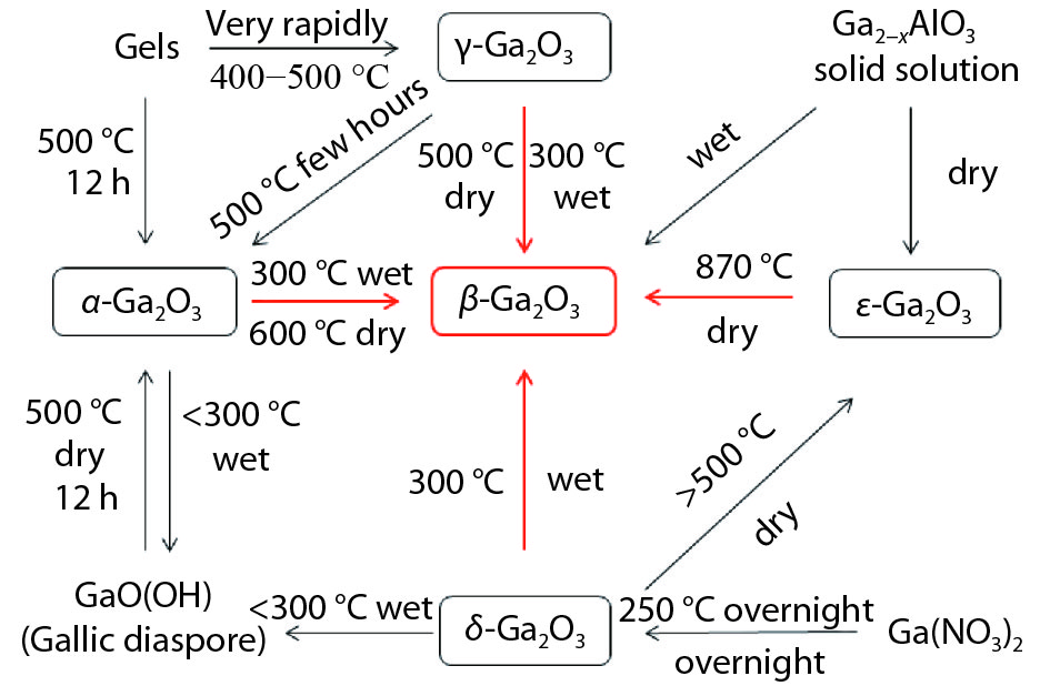
In fact, there have been five phases of Ga2O3, all of which can exist stably under normal condition and will convert into other phases at high pressures or high temperatures, as shown in Fig. 1[
![]()
Figure 1.(Color online) Transformation relationships among Ga2O3 in different crystalline phases and their hydrates[
β-Ga2O3 belongs to monoclinic system, C2/m space group, and its lattice constants are a = 1.22 nm, b = 0.3 nm, c = 0.58 nm, and β = 103.83°. The lattice constant value in the direction of (100) is much larger than those in (001) and (010), which means that it is easy to exfoliate the ultra-thin film from its (100) direction for device preparation. For the crystal structure, the double chain composed of [GaO6] octahedron is arranged along the b axis, and the chains are connected by [GaO4] tetrahedron. Ga atoms exists in the crystal in two kinds of forms of four and six ligands, as shown in Fig. 2[
![]()
Figure 2.(Color online) Crystal structure of
β-Ga2O3 has a large bandgap of approximately 4.8 eV and corresponding large estimated critical electric field strength of about 8 MV/cm, about twice that of SiC and GaN. The large bandgap of β-Ga2O3 allows its high temperature operation and the large critical field can sustain high voltage operation. However, the poor thermal conductivity of 0.1–0.3 W·cm−1·K−1 will limit high temperature capability of Ga2O3 based power devices and thermal management will be especially significant[
As the same as other wide bandgap materials, it is significant for β-Ga2O3 to control its electrical conductivity by doping or reduce defects in crystal. The n-type doping technology has been widely used in substrate, and epitaxial layer growth. Ion implantation has been used to reduce the contact resistance. Several common n-type dopants, such as Si, Ge and Sn, are proved to have low activation energy and can be effectively activated at room temperature. In addition, doping concentration can be flexibly modulated in the range of 1015–1019 cm−3, with the highest value of 1020 cm−3 reported[
Additionally, it’s worth noting that the future development of β-Ga2O3 needs to overcome the following two difficulties. (1) Develop effective p-type doping process, which determines the destiny of β-Ga2O3 based power electronics to some extent. It’s well-known that carrier inversion is the unique characteristic of semiconductor and reverse p-n junction can effectively undertake high voltage to give full play to the material advantages of β-Ga2O3. (2) Severe self-heating effects caused by the relatively low thermal conductivity of β-Ga2O3 must be mitigated in high voltage and high frequency application, though ultra-wide bandgap of β-Ga2O3 improve electronics thermal tolerance. What’s more, the mobility of carrier will also be reduced due to anabatic scatterings[
3. Field effect transistor based on β-Ga2O3
Summing up the above discussion, the physical properties suggest that β-Ga2O3 has a broad prospect in high voltage and high frequency power devices. At present, due to the absence of p-type doping, researchers focus on two kinds of unipolar devices, i.e. Schottky barrier diode (SBD) and field effect transistor (FET). FET is the conventional power switch device in which the resistance between source and drain electrodes is modulated by gate electrical field, and it is mainly used in converters and inverters.
The researching process of β-Ga2O3 based field effect transistors is shown in Fig. 3. Transistors develop from MESFET[
![]()
Figure 3.(Color online) The development of
In 2012, Higashiwaki et al. (from the National Institute of Information and Communications Technology (NICT)) manufactured a metal semiconductor field effect transistor (MESFET) on molecular-beam (MBE) epitaxial layer with Sn doping (7.0 × 1017 cm−3) on (010) oriental β-Ga2O3, as shown in Fig. 4(a)[
![]()
Figure 4.(Color online) Schematic cross-section of
Depletion-mode MOSFET with Vbr of 750 V was fabricated on MBE epitaxial (010) β-Ga2O3 layer with Sn doping of 3.0 × 1017 cm−3 by Wong et al. (from Novel Crystal Technology Inc.) in 2016, as shown in Fig. 5(a)[
![]()
Figure 5.(Color online) (a) Schematic cross-section, (b) the off-state drain/gate leakage and breakdown curves, (c) temperature-dependent transfer characteristics at
In 2016, Green et al. (from Wright-Patterson Air Force Base of USA) fabricated a depletion mode transistor on Sn doping (1.7 × 1018 cm−3) epitaxial layer of (100) oriental β-Ga2O3, which was grown via metal-organic vapor phase epitaxy (MOVPE). The transistor has a tremendous breakdown voltage of 230 V with a small gate-drain distance of 0.6 μm[
![]()
Figure 6.Top–down SEM image of the two-finger MOSFET on (100)
Though depletion-mode transistors show an excellent performance, including high current density, high breakdown voltage, low on-resistance etc, amounts of researches on enhancement-mode transistors have been also reported due to its unique advantages in application.
In 2016, a wrap-gate fin field-effect transistor operated on enhancement-mode was fabricated on (100) β-Ga2O3 by Chabak et al. (from Air Force Research Laboratory of USA). Fin array channels are beneficial for depletion by interface states to turn off without gate bias, but on current is limited to ~1 mA/mm[
![]()
Figure 7.(Color online) (a) SEM false-colored cross-section view of recessed-gate MOSFETs and HR-TEM of (b) its sidewall and (c) bottom facets of the gate-recess contact, (d) its gate-source and drain-source breakdown curves of both source-drain distances[
In March 2017, Wong et al. (from NICT) took advantage of fully depleted unintentionally doping (010) β-Ga2O3 (with a background carrier concentration of 4 × 1014 cm−3) to realize transistor’s operation in enhancement mode[
From the above, we can conclude that effective p-type doping is very significant for investigation of transistors. Without p–n junction structure, the thick gate dielectric is required to undertake too high voltage to excavate the excellent property of Ga2O3. In order to enhance breakdown voltage, vertical field effect transistor is a promising option.
In 2017, Wong et al. (from NICT) fabricated a vertical β-Ga2O3 MOSFET, and a buried current blocking layer (CBL) was used to electrically isolate the source and drain electrodes[
In 2017, Hu et al. (from Cornell University) attempted to fabricate vertical fin transistor, and though the device has an on/off ratio of 109, the field crowding near the bottom of the column limited Vbr to 185 V[
![]()
Figure 8.(Color online) (a) Schematic cross-section and SEM image, and (b) three-terminal off-state breakdown curves of vertical
In addition to high voltage, high theoretical electron velocity and high breakdown electrical field make β-Ga2O3 a potentially useful material in radio frequency (RF) and mm-wave region, and its power density at high frequency would not be limited by the low thermal conductivity. Therefore, some works in this direction have been reported in succession.
In 2017, Green et al. (from the Wright-Patterson Air Force Base of USA) used a highly doped cap layer to decrease contact resistance, and an incompletely depleted sub-micro gate recess to form modulation channel and attained a RF Ga2O3 transistor, as shown in Figs. 9(a) and 9(b)[
![]()
Figure 9.(Color online) (a) Cross section schematic, (b) focused ion beam (FIB) cross sectional image, and (c) extrinsic small signal RF gain performance of RF
The Ohio State University devoted themselves to utilize 2-dimensinal electron gas from silicon delta-doped β-Ga2O3 to fabricate high frequency transistors. In 2017, a delta-doping β-Ga2O3 MOSFET with integrated sheet charge of 2.4 × 1017 cm−2, mobility of 83 cm2V−1s−1, was manufactured by Krishnamoorthy et al., and drain current Imax of 236 mA/mm and transconducance gm of 26 mS/mm were obtained[
![]()
Figure 10.(Color online) (a) Schematic and (b) density-dependent field effect mobility of Silicon delta-doped
In addition, as mentioned above, β-Ga2O3 belongs to monoclinic system with the lattice of a axis longer than other two ones, and nano membrane can be acquired mechanically the same as 2-D materials[
![]()
Figure 11.(Color online) Depletion/enhancement-mode
4. Conclusion and future outlook
In conclusion, early researches on transistors mainly focus on realizing gate modulation and high breakdown voltage no matter planar and vertical structures. Up to now, the material properties of Ga2O3 have not been fully demonstrated experimentally, more investigations on p-type doping and device fabrications are in demand. In addition, low carrier mobility and self-heating effect are also research hotspots. There is no doubt that all efforts taken in FET will be beneficial for future improvement of Ga2O3 FET. Table 2 shows the basic performance parameters of some typical β-Ga2O3 based FETs reported up to now and apparently indicates their gradual improvement in performances. Based on the available achievements reported, we can summary that
(1) Al2O3 and SiO2 are widely used as gate insulators due to their larger conduction band offset with β-Ga2O3 and can effectively prevent gate leakage current. In addition, interfacial property in gate channel region affect the performance of FET, such as gate control ability and switch speed. Therefore, there are many studies focusing on evaluating and improving the interfacial property[
(2) High doping by ion implantation, spin-on-glass, or regrown layer are common methods to reduce contact resistance, and annealing can further improve Ohmic contact. Titanium is proved to be the best ohmic electrode metal directly contacting with β-Ga2O3[
(3) Depletion-mode transistors have been realized earlier. As for the enhancement-mode, either a low unintentional doping channel or a thin depletion layer by gate region interface states is proved to be effective solution when p-type doping is absent.
(4) The thermal damage should be unswervingly considered as the significant issue in β-Ga2O3 based power devices due to its relatively low thermal conductivity.
(5) The large theoretical breakdown electrical field of β-Ga2O3 can make a tradeoff between mobility and power loss during the high voltage and high frequency operation. In order to exert the advantages of β-Ga2O3, it’s necessary to scale down the gate length for high frequency application, and to develop vertical FETs for high voltage application.
Acknowledgements
This work was supported by the National Natural Science Foundation of China (Nos. 61521064, 61522408, 61574169, 61334007, 61474136, 61574166), the Ministry of Science and Technology of China (Nos. 2016YFA0201803, 2016YFA0203800, 2017YFB0405603), the Key Research Program of Frontier Sciences of Chinese Academy of Sciences (Nos. QYZDB-SSW-JSC048, QYZDY-SSW-JSC001), the Beijing Municipal Science and Technology Project (No. Z171100002017011), and the Opening Project of the Key Laboratory of Microelectronic Devices & Integration Technology, Institute of Microelectronics of Chinese Academy of Sciences
References
[1] J Millan, P Godignon, X Perpina et al. A survey of wide bandgap power semiconductor devices. IEEE Trans Power Electron, 29, 2155(2014).
[2]
[3] T P Chow, I Omura, M Higashiwaki et al. Smart power devices and ICs using GaAs and wide and extreme bandgap semiconductors. IEEE Trans Electron Devices, 64, 856(2017).
[4] S Fujita. Wide-bandgap semiconductor materials: For their full bloom. Jpn J Appl Phys, 54, 030101(2015).
[5] M Higashiwaki, K Sasaki, A Kuramata et al. Development of gallium oxide power device. Phys Status Solidi A, 211, 21(2014).
[6] M Higashiwaki, K Sasaki, H Murakami et al. Recent progress in Ga2O3 power devices. Semicond Sci Technol, 31, 034001(2016).
[7] N Ueda, H Hosono, R Waseda et al. Synthesis and control of conductivity of ultraviolet transmitting
[8] E G Víllora, K Shimamura, Y Yoshikawa et al. Large-size
[9] K N H Aida, H Takeda, N Aota et al. Growth of
[10] M Higashiwaki, K Konishi, K Sasaki et al. Temperature-dependent capacitance–voltage and current–voltage characteristics of Pt/Ga2O3 (001) Schottky barrier diodes fabricated on n-Ga2O3 drift layers grown by halide vapor phase epitaxy. Appl Phys Lett, 108, 133503(2016).
[11] M Higashiwaki, K Sasaki, T Kamimura et al. Depletion-mode Ga2O3 metal–oxide–semiconductor field-effect transistors on
[12] M Higashiwaki, K Sasaki, A Kuramata et al. Gallium oxide (Ga2O3) metal–semiconductor field-effect transistors on single-crystal
[13] W S Hwang, A Verma, H Peelaers et al. High-voltage field effect transistors with wide-bandgap
[14] Z Hu, K Nomoto, W Li et al. Enhancement-mode Ga2O3 vertical Transistors with breakdown voltage > 1 kV. IEEE Electron Device Lett, 39, 869(2018).
[15] K D Chabak, J P McCandless, N A Moser et al. Recessed-gate enhancement-mode
[16] M H Wong, K Sasaki, A Kuramata et al. Field-plated Ga2O3 MOSFETs with a breakdown voltage of over 750 V. IEEE Electron Device Lett, 37, 212-215(2016).
[17] H Zhou, M Si, S Alghamdi et al. High performance depletion/enhancement-mode
[18] Q He, W Mu, B Fu et al. Schottky barrier rectifier based on (100)
[19] K Sasaki, D Wakimoto, Q T Thieu et al. First demonstration of Ga2O3 trench MOS-type Schottky barrier diodes. IEEE Electron Device Lett, 38, 783(2017).
[20] K Konishi, K Goto, H Murakami et al. 1-kV vertical Ga2O3 field-plated Schottky barrier diodes. Appl Phys Lett, 110, 103506(2017).
[21] R Roy, V G Hill, E F Osborn. Polymorphism of Ga2O3 and the system Ga2O3–H2O. J Am Chem Soc, 74, 719(1952).
[22] H H Tippins. Optical absorption and photoconductivity in the band edge of
[23] T C Lovejoy, E N Yitamben, N Shamir et al. Surface morphology and electronic structure of bulk single crystal
[24] M Mohamed, C Janowitz, I Unger et al. The electronic structure of
[25] C Janowitz, V Scherer, M Mohamed et al. Experimental electronic structure of In2O3 and Ga2O3. New J Phys, 13, 085014(2011).
[26] O Ueda, N Ikenag, K Koshi et al. Structural evaluation of defects in
[27] F Mezzadri, G Calestani, F Boschi et al. Crystal structure and ferroelectric properties of epsilon-Ga2O3 films grown on (0001)-sapphire. Inorg Chem, 55, 2079(2016).
[28] X Xia, Y Chen, Q Feng et al. Hexagonal phase-pure wide band gap ε-Ga2O3 films grown on 6H-SiC substrates by metal organic chemical vapor deposition. Appl Phys Lett, 108, 202103(2016).
[29] M Slomski, N Blumenschein, P P Paskov et al. Anisotropic thermal conductivity of
[30] K Hoshikawa, E Oh, T Kobayashi et al. Growth of
[31] S Yoshioka, H Hayashi, A Kuwabara et al. Structures and energetics of Ga2O3 polymorphs. J Phys-Condens Mat, 19, 346211(2007).
[32] J Åhman, G Svensson, J Albertsson. A reinvestigation of beta-gallium oxide. Acta Crystallogr C, 52, 1336(1996).
[33] A Janotti, C G Van de Walle. Oxygen vacancies in ZnO. Appl Phys Lett, 87, 122102(2005).
[34] T Oshima, K Kaminaga, A Mukai et al. Formation of semi-insulating layers on semiconducting
[35] J B Varley, J R Weber, A Janotti et al. Oxygen vacancies and donor impurities in
[36] Z Hajnal, J Miró, G Kiss et al. Role of oxygen vacancy defect states in then-type conduction of
[37] J G M Fleischer, H Meixner. H2-induced changes in electrical conductance of
[38] F B C K A F M F C Kohl. Decomposition of methane on polycrystalline thick films of Ga2O3 investigated by thermal desorption spectroscopy with a mass spectrometer. Fresenius J Ana Chem, 358, 187(1997).
[39] M F T Schwebel, H Meixner, C D Kohl. CO-sensor for domestic use based on high temperature stable Ga2O3 thin films. Sens Actuators B Chem, 49, 46(1998).
[40] K H M Ogita, Y Nakanishi, Y Hatanaka. Ga2O3 thin film for oxygen sensor at high temperature. Appl Surf Sci, 175, 721(2001).
[41] Z Guo, A Verma, X Wu et al. Anisotropic thermal conductivity in single crystal
[42] M Handwerg, R Mitdank, Z Galazka et al. Temperature-dependent thermal conductivity in Mg-doped and undoped
[43] M D Santia, N Tandon, J D Albrecht. Lattice thermal conductivity in
[44]
[45]
[46] N Ma, N Tanen, A Verma et al. Intrinsic electron mobility limits in
[47] T Oishi, Y Koga, K Harada et al. High-mobility
[48] M Higashiwaki, A Kuramata, H Murakami et al. State-of-the-art technologies of gallium oxide power devices. J Phys D, 50, 333002(2017).
[49] C Tang, J Sun, N Lin et al. Electronic structure and optical property of metal-doped Ga2O3: a first principles study. RSC Adv, 6, 78322(2016).
[50] H Peelaers, C G Van de Walle. Brillouin zone and band structure of
[51] H von Wenckstern. Group-III sesquioxides: growth, physical properties and devices. Adv Electron Mater, 3, 1600350(2017).
[52] K Sasaki, M Higashiwaki, A Kuramata et al. MBE grown Ga2O3 and its power device applications. J Crys Growth, 378, 591(2013).
[53] M H Wong, Y Morikawa, K Sasaki et al. Characterization of channel temperature in Ga2O3 metal–oxide–semiconductor field-effect transistors by electrical measurements and thermal modeling. Appl Phys Lett, 109, 193503(2016).
[54]
[55] A J Green, K D Chabak, E R Heller et al. 3.8-MV/cm breakdown strength of MOVPE-grown Sn-doped
[56] M H Wong, Y Nakata, A Kuramata et al. Enhancement-mode Ga2O3 MOSFETs with Si-ion-implanted source and drain. Appl Phys Express, 10, 041101(2017).
[57]
[58]
[59] A J Green, K D Chabak, M Baldini et al.
[60] S Krishnamoorthy, Z Xia, S Bajaj et al. Delta-doped
[61] Z Xia, C Joishi, S Krishnamoorthy et al. Delta doped
[62]
[63] S Ahn, F Ren, J Kim et al. Effect of front and back gates on
[64] J Bae, H W Kim, I H Kang et al. High breakdown voltage quasi-two-dimensional
[65] H Zhou, K Maize, G Qiu et al.
[66] H Zhou, S Alghamdi, S W Si et al. Al2O3/
[67] T Kamimura, D Krishnamurthy, A Kuramata et al. Epitaxially grown crystalline Al2O3 interlayer on
[68] M Hattori, T Oshima, R Wakabayashi et al. Epitaxial growth and electric properties of γ-Al2O3 (110) films on
[69] K Zeng, Y Jia, U Singisetti. Interface state density in atomic layer deposited SiO2/
[70] K Zeng, U Singisetti. Temperature dependent quasi-static capacitance-voltage characterization of SiO2/
[71] H Dong, W Mu, Y Hu et al.
[72] M A Bhuiyan, H Zhou, R Jiang et al. Charge trapping in Al2O3/
[73] Y Yao, R F Davis, L M Porter. Investigation of different metals as ohmic contacts to
[74] N A Moser, J P McCandless, A Crespo et al. High pulsed current density
[75] K Sasaki, Q T Thieu, D Wakimoto et al. Depletion-mode vertical Ga2O3 trench MOSFETs fabricated using Ga2O3 homoepitaxial films grown by halide vapor phase epitaxy. Appl Phys Express, 10, 124201(2017).
[76] K Zeng, J S Wallace, C Heimburger et al. Ga2O3 MOSFETs using spin-on-glass source/drain doping technology. IEEE Electron Device Lett, 38, 513(2017).

Set citation alerts for the article
Please enter your email address
© Copyright 2018-2021 | Chinese Laser Press. All Rights Reserved 沪ICP备15018463号-20