• Photonics Research
  • Vol. 8, Issue 4, 601 (2020)
Kai Zou1、2, Yun Meng1、2, Zhao Wang1、2, and Xiaolong Hu1、2、*
Author Affiliations
  • 1School of Precision Instrument and Optoelectronic Engineering, Tianjin University, Tianjin 300072, China
  • 2Key Laboratory of Optoelectronic Information Science and Technology, Ministry of Education, Tianjin 300072, China
  • show less
    DOI: 10.1364/PRJ.380764 Cite this Article Set citation alerts
    Kai Zou, Yun Meng, Zhao Wang, Xiaolong Hu. Superconducting nanowire multi-photon detectors enabled by current reservoirs[J]. Photonics Research, 2020, 8(4): 601 Copy Citation Text show less
    Comparison between commonly used technology for N-fold coincidence photon counting with the proposed one using a superconducting nanowire multi-photon detector (SNMPD) presented in this paper. (a) A conventional N-fold coincidence photon counter requires N single-photon detectors as well as the associated electronics. (b) We propose to use a single SNMPD to count N-fold coincidence. SPD, single-photon detector; RF, radio frequency.
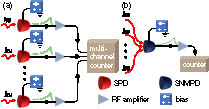
    Fig. 1. Comparison between commonly used technology for N-fold coincidence photon counting with the proposed one using a superconducting nanowire multi-photon detector (SNMPD) presented in this paper. (a) A conventional N-fold coincidence photon counter requires N single-photon detectors as well as the associated electronics. (b) We propose to use a single SNMPD to count N-fold coincidence. SPD, single-photon detector; RF, radio frequency.
    Schematic drawing of the device layout and the operating principle of the SNMPDs. (a) Device layout. The SNMPD is composed of N cascaded photosensitive superconducting nanowires (N1,N2,…,NN) and a wider one functioning as a current reservoir (R). See the main text for the definitions of Ib, Ib(0), Isw, Lk, Lc, α, β, and η. (b) Initial current distribution among the nanowires and the current reservoir. (c) Current redistribution after the first photosensitive nanowire N1 is fired by the first photon. (d) Current redistribution after the Nth photosensitive nanowire NN is fired by the Nth photon. The current reservoir R is also fired, and current is diverted into the load impedance Z0. (e) The bias conditions for the device to work as an N-photon detector as shown by the dashed lines. The open circles and triangles represent the upper bonds of Ib(0)/Isw, and the squares represent the lower bonds of Ib(0)/Isw. Note that the two sets of upper bounds (open circles and triangles) are identical.
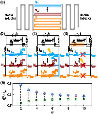
    Fig. 2. Schematic drawing of the device layout and the operating principle of the SNMPDs. (a) Device layout. The SNMPD is composed of N cascaded photosensitive superconducting nanowires (N1,N2,,NN) and a wider one functioning as a current reservoir (R). See the main text for the definitions of Ib, Ib(0), Isw, Lk, Lc, α, β, and η. (b) Initial current distribution among the nanowires and the current reservoir. (c) Current redistribution after the first photosensitive nanowire N1 is fired by the first photon. (d) Current redistribution after the Nth photosensitive nanowire NN is fired by the Nth photon. The current reservoir R is also fired, and current is diverted into the load impedance Z0. (e) The bias conditions for the device to work as an N-photon detector as shown by the dashed lines. The open circles and triangles represent the upper bonds of Ib(0)/Isw, and the squares represent the lower bonds of Ib(0)/Isw. Note that the two sets of upper bounds (open circles and triangles) are identical.
    Electrothermal dynamics of a superconducting nanowire two-photon detector. Panel (a) presents the electrothermal evolution after the first photon is absorbed by the first photosensitive nanowire at t=0; (a1), (a2), and (a3) present the current-temperature phase diagrams of the first and the second photosensitive nanowires and the current reservoir, respectively. Panel (b) presents the electrothermal evolution after the second photon is absorbed by the second photosensitive nanowire at t=10 ns; (b1), (b2), and (b3) present the current-temperature phase diagrams of the first and second photosensitive nanowires and the current reservoir, respectively. In the phase diagrams, the open circles and solid dots present the initial and the final states, respectively, of the corresponding photon-detection event. The dotted lines in (a1) and (b2) represent the abrupt changes on the phase diagrams due to photon excitations, whereas the solid lines in (a1), (a2), (a3), (b1), (b2), and (b3) represent the continuous electrothermal evolutions of the nanowires after photon excitations. The black dashed lines separate the superconducting phase (S) and the normal phase (N) of the nanowires. The insets present the corresponding spatial-temporal diagrams of the temperature distribution. (c) Current dynamics of I1(t), I2(t), IR(t), and Iout(t) (see Visualization 1).
    Fig. 3. Electrothermal dynamics of a superconducting nanowire two-photon detector. Panel (a) presents the electrothermal evolution after the first photon is absorbed by the first photosensitive nanowire at t=0; (a1), (a2), and (a3) present the current-temperature phase diagrams of the first and the second photosensitive nanowires and the current reservoir, respectively. Panel (b) presents the electrothermal evolution after the second photon is absorbed by the second photosensitive nanowire at t=10  ns; (b1), (b2), and (b3) present the current-temperature phase diagrams of the first and second photosensitive nanowires and the current reservoir, respectively. In the phase diagrams, the open circles and solid dots present the initial and the final states, respectively, of the corresponding photon-detection event. The dotted lines in (a1) and (b2) represent the abrupt changes on the phase diagrams due to photon excitations, whereas the solid lines in (a1), (a2), (a3), (b1), (b2), and (b3) represent the continuous electrothermal evolutions of the nanowires after photon excitations. The black dashed lines separate the superconducting phase (S) and the normal phase (N) of the nanowires. The insets present the corresponding spatial-temporal diagrams of the temperature distribution. (c) Current dynamics of I1(t), I2(t), IR(t), and Iout(t) (see Visualization 1).
    Bias conditions for the detector functioning as an n-photon detector, where n=1,2,…,N; (a) and (b) present the same data set in two different ways. (a) The bias regions with the maximum photon numbers for each N (n=N), with the second largest photon numbers for each N (n=N-1), and so on. (b) The bias regions for a given photon number n, for example, n=1,2,….
    Fig. 4. Bias conditions for the detector functioning as an n-photon detector, where n=1,2,,N; (a) and (b) present the same data set in two different ways. (a) The bias regions with the maximum photon numbers for each N (n=N), with the second largest photon numbers for each N (n=N-1), and so on. (b) The bias regions for a given photon number n, for example, n=1,2,.
    Comparison within bias conditions for an N-SNAP (black symbols), an SNMPD with α=N (red symbols), and an SNMPD with α=2N (blue symbols).
    Fig. 5. Comparison within bias conditions for an N-SNAP (black symbols), an SNMPD with α=N (red symbols), and an SNMPD with α=2N (blue symbols).
    Current dynamics of a superconducting nanowire eight-photon detector. (a) Current dynamics of the eight photosensitive nanowires, (b) current dynamics of the reservoir, (c) the output voltage pulse on the load impedance without external amplification. The dashed lines in (a) and (b) present the switching currents.
    Fig. 6. Current dynamics of a superconducting nanowire eight-photon detector. (a) Current dynamics of the eight photosensitive nanowires, (b) current dynamics of the reservoir, (c) the output voltage pulse on the load impedance without external amplification. The dashed lines in (a) and (b) present the switching currents.
    Operation of a superconducting nanowire eight-photon detector in the six-photon regime. (a) Current dynamics of the eight photosensitive nanowires, (b) current dynamics of the reservoir, (c) the output voltage pulse on the load impedance without external amplification. The dashed lines in (a) and (b) present the switching currents.
    Fig. 7. Operation of a superconducting nanowire eight-photon detector in the six-photon regime. (a) Current dynamics of the eight photosensitive nanowires, (b) current dynamics of the reservoir, (c) the output voltage pulse on the load impedance without external amplification. The dashed lines in (a) and (b) present the switching currents.
    η as a function of Ib(0)/Isw, obtained by electrothermal simulation, for a superconducting nanowire two-photon detector. For the first photon, η is slightly below 0.8; for the second photon, η is slightly above 0.8.
    Fig. 8. η as a function of Ib(0)/Isw, obtained by electrothermal simulation, for a superconducting nanowire two-photon detector. For the first photon, η is slightly below 0.8; for the second photon, η is slightly above 0.8.
    Comparison between bias conditions obtained analytically (solid symbols) and bias conditions obtained by SPICE simulation (open symbols).
    Fig. 9. Comparison between bias conditions obtained analytically (solid symbols) and bias conditions obtained by SPICE simulation (open symbols).
    Waveguide-integrated superconducting nanowire multi-photon detector.
    Fig. 10. Waveguide-integrated superconducting nanowire multi-photon detector.
    Kai Zou, Yun Meng, Zhao Wang, Xiaolong Hu. Superconducting nanowire multi-photon detectors enabled by current reservoirs[J]. Photonics Research, 2020, 8(4): 601
    Download Citation