• Opto-Electronic Advances
  • Vol. 1, Issue 5, 180009-1 (2018)
Arash Nemati1、2, Qian Wang1, Minghui Hong2, and Jinghua Teng1、*
Author Affiliations
  • 1Institute of Materials Research & Engineering, Agency for Science, Technology and Research (A*STAR), 2 Fusionopolis Way, Singa-pore 138634, Singapore
  • 2Department of Electrical and Computer Engineering, National University of Singapore, Singapore 117576, Singapore
  • show less
    DOI: 10.29026/oea.2018.180009 Cite this Article
    Arash Nemati, Qian Wang, Minghui Hong, Jinghua Teng. Tunable and reconfigurable metasurfaces and metadevices[J]. Opto-Electronic Advances, 2018, 1(5): 180009-1 Copy Citation Text show less
    Schematic art view of the different mechanisms in tunable metasurfaces.
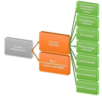
    Fig. 1. Schematic art view of the different mechanisms in tunable metasurfaces.
    The metal-oxide-semiconductor heterostructure with ITO as the active material. Figure reproduced from ref.119, American Chemical Society.
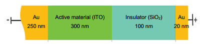
    Fig. 2. The metal-oxide-semiconductor heterostructure with ITO as the active material. Figure reproduced from ref.119, American Chemical Society.
    The refractive index (n) and extinction coefficient (k) in a 5 nm accumulation layer, extracted data from the ellipsometry measurements. Figure reproduced from ref.119, American Chemical Society.
    Fig. 3. The refractive index (n) and extinction coefficient (k) in a 5 nm accumulation layer, extracted data from the ellipsometry measurements. Figure reproduced from ref.119, American Chemical Society.
    The tunability of ITO in a multilayer modulator.(a) Cross section of the multilayer ITO modulator. (b) Picture of the fabricated modulator. (c) Solid and dashed lines are from further fitting by the Drude model. Figure reproduced from ref.120, Optical Society of America.
    Fig. 4. The tunability of ITO in a multilayer modulator. (a) Cross section of the multilayer ITO modulator. (b) Picture of the fabricated modulator. (c) Solid and dashed lines are from further fitting by the Drude model. Figure reproduced from ref.120, Optical Society of America.
    Tunable metasurfaces using ITO as an active layer.(a) Schematic of the tunable metasurface which consists of a quartz substrate, gold backplane, and a thin ITO film followed by a thin alumina film on which gold stripe nanoantenna array is patterned on. (b) Measured relative reflectance change from the metasurface for different applied voltages. (c) Measured and simulated phase shift as a function of applied bias for the applied voltage. The black lines show the cross-section for analyzing the phase. (d) Device schematic showing an electrically-tunable ITO film clamped between an HfO2-coated Au substrate and an array of Au strips. With positive and negative electric biases, the carrier concentration of ITO can be decreased (depletion) or increased (accumulation), leading to changes in the optical properties of the ITO. (e) Reflectance spectra were taken from the device measured using an FT-IR microscope. The red, blue, and green curves denote the reflectance spectra under 0 V for no bias, −5 V for accumulation, and +5 V for depletion, respectively. The grey curves represent reflectance spectra for intermediate voltages with an incremental step size of 1 V. (f) Schematic structure of the meta-molecule and (g) top-view small-scale SEM image of the metamaterial. (h) Measured reflectance changes of a 1550 nm probe laser as a function of delay time between pump and probe pulses. The red solid line is the exponential fit to the data. (i) The calculated reflectance spectrum of the metamaterial with different pump intensity by the finite element method. Figure reproduced from: (a–c) ref.47, American Chemical Society; (d, e) ref.85, Creative Commons Attribution 4.0 International License; (f–i) ref.59, Creative Commons Attribution 4.0 International License.
    Fig. 5. Tunable metasurfaces using ITO as an active layer. (a) Schematic of the tunable metasurface which consists of a quartz substrate, gold backplane, and a thin ITO film followed by a thin alumina film on which gold stripe nanoantenna array is patterned on. (b) Measured relative reflectance change from the metasurface for different applied voltages. (c) Measured and simulated phase shift as a function of applied bias for the applied voltage. The black lines show the cross-section for analyzing the phase. (d) Device schematic showing an electrically-tunable ITO film clamped between an HfO2-coated Au substrate and an array of Au strips. With positive and negative electric biases, the carrier concentration of ITO can be decreased (depletion) or increased (accumulation), leading to changes in the optical properties of the ITO. (e) Reflectance spectra were taken from the device measured using an FT-IR microscope. The red, blue, and green curves denote the reflectance spectra under 0 V for no bias, −5 V for accumulation, and +5 V for depletion, respectively. The grey curves represent reflectance spectra for intermediate voltages with an incremental step size of 1 V. (f) Schematic structure of the meta-molecule and (g) top-view small-scale SEM image of the metamaterial. (h) Measured reflectance changes of a 1550 nm probe laser as a function of delay time between pump and probe pulses. The red solid line is the exponential fit to the data. (i) The calculated reflectance spectrum of the metamaterial with different pump intensity by the finite element method. Figure reproduced from: (a–c) ref.47, American Chemical Society; (d, e) ref.85, Creative Commons Attribution 4.0 International License; (f–i) ref.59, Creative Commons Attribution 4.0 International License.
    Phase transition in ferroelectric materials.(a) Temperature dependence of the dielectric constant of a ferroelectric material. The material transitions from a polar to a non-polar phase at the Curie temperature Tc. (b, c) The corresponding polarization and dielectric constant as a function of applied field below and above Tc. Figure reproduced from: (a–c) ref.124, AIP Publishing.
    Fig. 6. Phase transition in ferroelectric materials. (a) Temperature dependence of the dielectric constant of a ferroelectric material. The material transitions from a polar to a non-polar phase at the Curie temperature Tc. (b, c) The corresponding polarization and dielectric constant as a function of applied field below and above Tc. Figure reproduced from: (a–c) ref.124, AIP Publishing.
    Thermal tuning of ferroelectric materials in active metamaterials.(a) Microscopic image of the metamaterial consisting of a gold electric split-ring resonator array fabricated on an STO substrate and (b) measured normalized THz transmission amplitude spectra through the metamaterial. (c) and (e) show the unit cell of the proposed frequency tunable metallic ring and cross absorbers, respectively and (d) and (f) show the calculated absorption spectra of the proposed frequency tunable metallic ring and cross absorbers at different temperatures, respectively. (g) Schematic view of the structure. (h) Scanning electron microscopy image of the metamaterial. (i) Theoretical and experimental transmission spectra. Figure reproduced from: (a, b) ref.52, Optical Society of America; (c–f) ref.53, Optical Society of America; (g–i) ref.130, Springer Nature.
    Fig. 7. Thermal tuning of ferroelectric materials in active metamaterials.

    (a) Microscopic image of the metamaterial consisting of a gold electric split-ring resonator array fabricated on an STO substrate and (b) measured normalized THz transmission amplitude spectra through the metamaterial. (c) and (e) show the unit cell of the proposed frequency tunable metallic ring and cross absorbers, respectively and (d) and (f) show the calculated absorption spectra of the proposed frequency tunable metallic ring and cross absorbers at different temperatures, respectively. (g) Schematic view of the structure. (h) Scanning electron microscopy image of the metamaterial. (i) Theoretical and experimental transmission spectra. Figure reproduced from: (a, b) ref.52, Optical Society of America; (c–f) ref.53, Optical Society of America; (g–i) ref.130, Springer Nature.

    Electrical tuning of the ferroelectric material in active metamaterials.(a) Schematic view of the SRR unit cell and the IDE patterns. (b) SEM image of the SRRs and the IDE patterns. (c) Transmission spectra of the metamaterial at various electric fields. (d) Schematic illustration of the metamaterial and experimental design. (e) Microscopic image of the fabricated BST–silicon hybrid metamaterial. (f) Measured transmission amplitude spectra of the BST–silicon hybrid metamaterial at various gate currents. Figure reproduced from: (a–c) ref.51, AIP Publishing; (d–f) ref.139, John Wiley and Sons.
    Fig. 8. Electrical tuning of the ferroelectric material in active metamaterials. (a) Schematic view of the SRR unit cell and the IDE patterns. (b) SEM image of the SRRs and the IDE patterns. (c) Transmission spectra of the metamaterial at various electric fields. (d) Schematic illustration of the metamaterial and experimental design. (e) Microscopic image of the fabricated BST–silicon hybrid metamaterial. (f) Measured transmission amplitude spectra of the BST–silicon hybrid metamaterial at various gate currents. Figure reproduced from: (a–c) ref.51, AIP Publishing; (d–f) ref.139, John Wiley and Sons.
    Tunable metamaterials using graphene as the active material.(a) Schematic view of the ultrathin optical modulator based on a tunable metasurface absorber. (b) SEM image of the metasurface on graphene (a zoomed-in view of a portion of the metasurface is shown in the inset). (c) Normalized measured reflection spectra of the metasurface absorber for different gate voltages (VG−VCNP=VCNP is the gate voltage when the concentrations of electrons and holes in the graphene sheet are equal) to the reflection spectra from a 300 nm Al film on the same silicon substrate. Schematic (d) top and (e) side view of a typical graphene micro-ribbon array on a Si/SiO2 substrate, (f) AFM image of a graphene micro-ribbon array sample with a ribbon width of 4 mm and a ribbon and gap width ratio of 1:1, and (g) relative mid-infrared transmission spectra (T/TCNP) of the graphene ribbon array as gate voltage (Vg−VCNP) varies from-0.3 to 2.2 V (the voltages corresponding to the un-labeled lines, starting with the red line and alternating downwards, are 2.0 V, 1.6 V, 1.2 V, 0.7 V and 0.3 V). (h) Schematic view of the composite multilayer material made by stacking graphene sheets and dielectric layers (under certain conditions, it exhibits hyperbolic-like iso-frequency wavevector dispersion which is shown in the inset, where Vg indicates the direction of the group velocity), (i) reflection and (j) transmission for a finite thickness graphene-silica multilayered HM, at normal polarization, calculated by transfer matrix method (solid lines) and EMA (circles) when graphene layers are unbiased, i.e., μc=0 eV, and (k) reflection and (l) transmission versus frequency, for the same set of parameters, except that now graphene layers are biased with μc=0.4 eV. Figure reproduced from: (a–c) ref.88, American Chemical Society; (d–g) ref.49, Springer Nature; (i–l) ref.162, Optical Society of America.
    Fig. 9. Tunable metamaterials using graphene as the active material.

    (a) Schematic view of the ultrathin optical modulator based on a tunable metasurface absorber. (b) SEM image of the metasurface on graphene (a zoomed-in view of a portion of the metasurface is shown in the inset). (c) Normalized measured reflection spectra of the metasurface absorber for different gate voltages (VGVCNP=VCNP is the gate voltage when the concentrations of electrons and holes in the graphene sheet are equal) to the reflection spectra from a 300 nm Al film on the same silicon substrate. Schematic (d) top and (e) side view of a typical graphene micro-ribbon array on a Si/SiO2 substrate, (f) AFM image of a graphene micro-ribbon array sample with a ribbon width of 4 mm and a ribbon and gap width ratio of 1:1, and (g) relative mid-infrared transmission spectra (T/TCNP) of the graphene ribbon array as gate voltage (VgVCNP) varies from-0.3 to 2.2 V (the voltages corresponding to the un-labeled lines, starting with the red line and alternating downwards, are 2.0 V, 1.6 V, 1.2 V, 0.7 V and 0.3 V). (h) Schematic view of the composite multilayer material made by stacking graphene sheets and dielectric layers (under certain conditions, it exhibits hyperbolic-like iso-frequency wavevector dispersion which is shown in the inset, where Vg indicates the direction of the group velocity), (i) reflection and (j) transmission for a finite thickness graphene-silica multilayered HM, at normal polarization, calculated by transfer matrix method (solid lines) and EMA (circles) when graphene layers are unbiased, i.e., μc=0 eV, and (k) reflection and (l) transmission versus frequency, for the same set of parameters, except that now graphene layers are biased with μc=0.4 eV. Figure reproduced from: (a–c) ref.88, American Chemical Society; (d–g) ref.49, Springer Nature; (i–l) ref.162, Optical Society of America.

    Tunable metamaterials using GST as the active material.(a) Schematic diagram of the plasmonic metamaterial which has an array of gold nano-disks on a thin layer of GST (T=40 nm, t=20 nm, d=280 nm, a=1.2 µm). (b) Measured normalized transmission spectra of continuously tuning of the hybrid plasmonic metamaterial measured at different baking time during the crystallization process. (c) The schematic view of the active plasmonic metasurface for beam switching which consists of a 50 nm thick GST-326 layer underneath a geometric phase metasurface for beam switching (two types of nano-antennas A and B with different plasmon resonances are alternated line-wise), when the active layer is in the amorphous phase, only type A rods interact with the incident light and deviate the beam to the left and when the active layer is in the crystalline phase, only type B rods interact with the incident light and deviate the beam into the opposite direction due to their relative orientation (right). (d) Infrared camera images and intensity plots of the beam transmitted by the active metasurface in the amorphous (left) and crystalline (right) state. (e) Schematic view of switchable THz quarter-wave plate design. The top left inset is a microscope image of one unit cell in the fabricated sample (P=150, Lx=90, Ly=124, lx=9, ly=5 and w=9 μm, and the scale bar is 50 μm). The top right inset is the simulated ellipticities of the output THz waves. (f) Schematic backside view of the resistive heater with a square aperture (6 mm × 6 mm) milled at the center to allow THz to pass through. (g) Measured transmission spectra along two slots at 300 K (solid line) and 400 K (dot line). (h) Measured the phase difference between y- and x-axes at 300 K (solid line) and 400 K (dot line). Figure reproduced from: (a, b) ref.92, Optical Society of America; (c, d) ref.167, Creative Commons Attribution 4.0 International License; (e–h) ref.96, Creative Commons Attribution 4.0 International License.
    Fig. 10. Tunable metamaterials using GST as the active material. (a) Schematic diagram of the plasmonic metamaterial which has an array of gold nano-disks on a thin layer of GST (T=40 nm, t=20 nm, d=280 nm, a=1.2 µm). (b) Measured normalized transmission spectra of continuously tuning of the hybrid plasmonic metamaterial measured at different baking time during the crystallization process. (c) The schematic view of the active plasmonic metasurface for beam switching which consists of a 50 nm thick GST-326 layer underneath a geometric phase metasurface for beam switching (two types of nano-antennas A and B with different plasmon resonances are alternated line-wise), when the active layer is in the amorphous phase, only type A rods interact with the incident light and deviate the beam to the left and when the active layer is in the crystalline phase, only type B rods interact with the incident light and deviate the beam into the opposite direction due to their relative orientation (right). (d) Infrared camera images and intensity plots of the beam transmitted by the active metasurface in the amorphous (left) and crystalline (right) state. (e) Schematic view of switchable THz quarter-wave plate design. The top left inset is a microscope image of one unit cell in the fabricated sample (P=150, Lx=90, Ly=124, lx=9, ly=5 and w=9 μm, and the scale bar is 50 μm). The top right inset is the simulated ellipticities of the output THz waves. (f) Schematic backside view of the resistive heater with a square aperture (6 mm × 6 mm) milled at the center to allow THz to pass through. (g) Measured transmission spectra along two slots at 300 K (solid line) and 400 K (dot line). (h) Measured the phase difference between y- and x-axes at 300 K (solid line) and 400 K (dot line). Figure reproduced from: (a, b) ref.92, Optical Society of America; (c, d) ref.167, Creative Commons Attribution 4.0 International License; (e–h) ref.96, Creative Commons Attribution 4.0 International License.
    Liquid crystal molecules orientation and periodicity in (a) smectic, (b) nematic, and (c) isotropic phases.
    Fig. 11. Liquid crystal molecules orientation and periodicity in (a) smectic, (b) nematic, and (c) isotropic phases.
    Tunable metamaterials using LCs as the active material.(a) Schematic of the sample structure and experimental setup. The inset Ⅰ shows the fabricated square pattern of gold AAAs. The inset Ⅱ shows the working mechanism of the optical driving process. The (b) theoretically calculated and (c) experimentally measured transmission spectra of color filters with different aperture sizes. The inset in (c) shows the measured FWHM of corresponding transmission peaks. (d) The evolution of the transmission spectra as a function of time under the UV pump for the color filter with an aperture size of 120 nm. (e) Schematic view of metamaterial absorber array covered with LC designed for the experiment. (f) Comparison of the measured frequency-dependent absorptivities (A=1−R) in the biased (red continuous line) and unbiased conditions (blue continuous line) with those from numerical calculations (dashed lines). The inset shows the calculated percentage modulation factor as a function of the liquid crystal losses. (g) Schematic view of the silicon nanodisk metasurface integrated into an LC cell. The silicon nanodisk sample is immersed in the LC, and the cell is covered by a layer of brushed PVA for alignment of the LC. A resistor heater is mounted on the backside of the silicon wafer. (h) Scanning electron micrograph of the silicon nanodisk metasurface. (i) Measured normalized transmittance spectra. (j) Schematic illustration of gold nanorods alignment in the nematic LC and (k) gold nanorods alignment in a columnar hexagonal lyotropic LC phase. (l) Experimental extinction spectra of gold nanorods in a nematic LC realigned by a magnetic field. Figure reproduced from: (a–d) ref.101, John Wiley and Sons; (e, f) ref.108, John Wiley and Sons; (g–i) ref.109, American Chemical Society; (j–l) ref.67, American Chemical Society.
    Fig. 12. Tunable metamaterials using LCs as the active material. (a) Schematic of the sample structure and experimental setup. The inset Ⅰ shows the fabricated square pattern of gold AAAs. The inset Ⅱ shows the working mechanism of the optical driving process. The (b) theoretically calculated and (c) experimentally measured transmission spectra of color filters with different aperture sizes. The inset in (c) shows the measured FWHM of corresponding transmission peaks. (d) The evolution of the transmission spectra as a function of time under the UV pump for the color filter with an aperture size of 120 nm. (e) Schematic view of metamaterial absorber array covered with LC designed for the experiment. (f) Comparison of the measured frequency-dependent absorptivities (A=1−R) in the biased (red continuous line) and unbiased conditions (blue continuous line) with those from numerical calculations (dashed lines). The inset shows the calculated percentage modulation factor as a function of the liquid crystal losses. (g) Schematic view of the silicon nanodisk metasurface integrated into an LC cell. The silicon nanodisk sample is immersed in the LC, and the cell is covered by a layer of brushed PVA for alignment of the LC. A resistor heater is mounted on the backside of the silicon wafer. (h) Scanning electron micrograph of the silicon nanodisk metasurface. (i) Measured normalized transmittance spectra. (j) Schematic illustration of gold nanorods alignment in the nematic LC and (k) gold nanorods alignment in a columnar hexagonal lyotropic LC phase. (l) Experimental extinction spectra of gold nanorods in a nematic LC realigned by a magnetic field. Figure reproduced from: (a–d) ref.101, John Wiley and Sons; (e, f) ref.108, John Wiley and Sons; (g–i) ref.109, American Chemical Society; (j–l) ref.67, American Chemical Society.
    Tunable metamaterials using semiconductors as the active material.(a) Top and (b) side view SEM images of the fabricated InSb grating and (c) Schematic of the transmission measurement configuration used in FTIR. Measured transmittances of (d) TM and (e) TE polarized THz waves through samples with and without laser excitations. (f) Geometry and dimensions of the THz metamaterial resonator (A=36 μm, G=2 μm, D=10 μm, and W=4 μm). (g) The metamaterial unit cells are connected together with metal wires to serve as a metallic (Schottky) gate. (h) The strength of the resonance is controlled by tuning the substrate charge carrier density near the split gaps which is relative to the voltage bias applied between the Schottky and ohmic contacts (the grey scale indicates the free charge carrier density). (i) Measured transmitted intensity of THz radiation, and (j) the corresponding permittivity for various gate voltage bias. Figure reproduced from: (a–e) ref.58, Licensed Content Publisher; (f–j) ref.107, Springer Nature.
    Fig. 13. Tunable metamaterials using semiconductors as the active material. (a) Top and (b) side view SEM images of the fabricated InSb grating and (c) Schematic of the transmission measurement configuration used in FTIR. Measured transmittances of (d) TM and (e) TE polarized THz waves through samples with and without laser excitations. (f) Geometry and dimensions of the THz metamaterial resonator (A=36 μm, G=2 μm, D=10 μm, and W=4 μm). (g) The metamaterial unit cells are connected together with metal wires to serve as a metallic (Schottky) gate. (h) The strength of the resonance is controlled by tuning the substrate charge carrier density near the split gaps which is relative to the voltage bias applied between the Schottky and ohmic contacts (the grey scale indicates the free charge carrier density). (i) Measured transmitted intensity of THz radiation, and (j) the corresponding permittivity for various gate voltage bias. Figure reproduced from: (a–e) ref.58, Licensed Content Publisher; (f–j) ref.107, Springer Nature.
    Flexible tunable metamaterials made on elastic substrates.(a) FTIR reflection spectra for the metamaterial with a coupling distance of 60 nm are shown. The inset shows SEM image of the fabricated sample. Image of (b) 2D planar metamaterial and (c) 3D terahertz metamaterial tube at a diameter of 4.00 mm. (d) Resonance frequency shifts as a function of core diameter for the hollow- and solid-core (cotton and paper) metamaterials tubes. SEM image of (e) the nano-posts before spin coating the first PDMS layer and (f) the nano-posts embedded in the PDMS. (g) Measured and analytically predicted focal distances (i.e. (1+ε)2×f) for different strain values versus the square of the stretch ratio ((1+ε)2). (h) A side view schematic illustration of a dielectric metasurface microlens that by stretching with a stretch ratio of (1+ε), the focal distance changes by (1+ε)2. (i) Schematic illustration of the metasurface hologram on the PDMS substrate. (j) and (k) Experimentally measured hologram images at an image plane 200 μm from the metasurface for a device that is not stretched and stretched. (l) Experimentally captured hologram images at a distance of 340 μm from the metasurface when the device is unstretched, stretched 112%, and 130%. Figure reproduced from: (a) ref.230, American Chemical Society; (b–d) ref.72, John Wiley and Sons; (e–h) ref.70, John Wiley and Sons; (i–l) ref.231, American Chemical Society.
    Fig. 14. Flexible tunable metamaterials made on elastic substrates. (a) FTIR reflection spectra for the metamaterial with a coupling distance of 60 nm are shown. The inset shows SEM image of the fabricated sample. Image of (b) 2D planar metamaterial and (c) 3D terahertz metamaterial tube at a diameter of 4.00 mm. (d) Resonance frequency shifts as a function of core diameter for the hollow- and solid-core (cotton and paper) metamaterials tubes. SEM image of (e) the nano-posts before spin coating the first PDMS layer and (f) the nano-posts embedded in the PDMS. (g) Measured and analytically predicted focal distances (i.e. (1+ε)2×f) for different strain values versus the square of the stretch ratio ((1+ε)2). (h) A side view schematic illustration of a dielectric metasurface microlens that by stretching with a stretch ratio of (1+ε), the focal distance changes by (1+ε)2. (i) Schematic illustration of the metasurface hologram on the PDMS substrate. (j) and (k) Experimentally measured hologram images at an image plane 200 μm from the metasurface for a device that is not stretched and stretched. (l) Experimentally captured hologram images at a distance of 340 μm from the metasurface when the device is unstretched, stretched 112%, and 130%. Figure reproduced from: (a) ref.230, American Chemical Society; (b–d) ref.72, John Wiley and Sons; (e–h) ref.70, John Wiley and Sons; (i–l) ref.231, American Chemical Society.
    Reconfigurable metamaterials using M-NEMS. SEM image of (a) the metamaterial molecule array with micro-machined actuators and (b) the close-up top view of the unit cell. The measured reflection coefficient of the metamaterial under the TE polarized incidence in (c) the open-ring state (G=2 μm, 4 μm, and 6 μm), (d) the closed-ring state, and (e) the back-touch state (The simulation results of the induced surface currents by the magnetic response is shown on the right side of each figure). SEM image of (f) the metamaterial molecule array with micro-machined actuators and (g) the close-up top view of the unit cell. The simulated and measured transmission spectra for the TM polarization incident wave at (h) Δ =0, (i) Δ =2.5, 5, 10, 15 μm (from dark to light), and (j) Δ =20 μm. The simulated surface currents and normal magnetic field components are shown on the right side of each figure. (k) SEM image of the fabricated metamaterial (the zoom-in image of the omega-ring design is shown in the inset), (l) Cross-sectional view of released omega-ring showing the angle of curvature (θ) and bending height (δ). (m) and (n) Measured transmission spectra of Omega-ring metamaterial in the TE-polarized and TM-polarized incidence when the voltage bias is 5 V, respectively. (o) SEM image of the reconfigurable plasmonic metamaterial. (p) Schematic of the driving circuit (black) and a section of the metamaterial pattern consisting of a gold nanostructure (yellow) supported by silicon nitride strings (brown). (q) Transmission and (r) reflection spectra of the metamaterial for different static voltages. Figure reproduced from: (a–e) ref.76, John Wiley and Sons; (f–j) ref.74, John Wiley and Sons; (k–n) ref.77, AIP Publishing; (o–r) ref.48, Springer Nature.
    Fig. 15. Reconfigurable metamaterials using M-NEMS. SEM image of (a) the metamaterial molecule array with micro-machined actuators and (b) the close-up top view of the unit cell. The measured reflection coefficient of the metamaterial under the TE polarized incidence in (c) the open-ring state (G=2 μm, 4 μm, and 6 μm), (d) the closed-ring state, and (e) the back-touch state (The simulation results of the induced surface currents by the magnetic response is shown on the right side of each figure). SEM image of (f) the metamaterial molecule array with micro-machined actuators and (g) the close-up top view of the unit cell. The simulated and measured transmission spectra for the TM polarization incident wave at (h) Δ =0, (i) Δ =2.5, 5, 10, 15 μm (from dark to light), and (j) Δ =20 μm. The simulated surface currents and normal magnetic field components are shown on the right side of each figure. (k) SEM image of the fabricated metamaterial (the zoom-in image of the omega-ring design is shown in the inset), (l) Cross-sectional view of released omega-ring showing the angle of curvature (θ) and bending height (δ). (m) and (n) Measured transmission spectra of Omega-ring metamaterial in the TE-polarized and TM-polarized incidence when the voltage bias is 5 V, respectively. (o) SEM image of the reconfigurable plasmonic metamaterial. (p) Schematic of the driving circuit (black) and a section of the metamaterial pattern consisting of a gold nanostructure (yellow) supported by silicon nitride strings (brown). (q) Transmission and (r) reflection spectra of the metamaterial for different static voltages. Figure reproduced from: (a–e) ref.76, John Wiley and Sons; (f–j) ref.74, John Wiley and Sons; (k–n) ref.77, AIP Publishing; (o–r) ref.48, Springer Nature.
    Operation spectrumModulation speedTuning MechanismTuning range/depthReference
    Transparent conductive oxidesVisible10 MHzElectrical30%47
    172 kHzElectrical15%85
    FerroelectricsGHz to visibleNAElectrical19%264
    NAThermal43%52
    NAOptical1.50%61
    Two dimensional (2D) materialsTHz to visible100 kHzElectrical47%50
    20 GHzElectrical95%88
    40 MHzElectrical60%151
    Phase change materialsTHz to visible294 MHzOptical16%172
    2.77 GHzOptical42%168
    312 MHzOptical46%175
    Liquid Crystals (LCs)GHz to visibleNAThermal15%103
    NAOptical18%101
    20 HzElectrical15%200
    SemiconductorsTHz to visibleNAElectrical79%139
    1.2 GHzOptical46.70%58
    Elastic materialsGHz to visibleNAMechanical8%233
    NAMechanical50.60%72
    M-NEMSGHz to visible1 kHzElectrical7.50%76
    1 kHzElectrical31%74
    1.5 kHzElectrical87%81
    Table 1. Comparison of different methods.
    Arash Nemati, Qian Wang, Minghui Hong, Jinghua Teng. Tunable and reconfigurable metasurfaces and metadevices[J]. Opto-Electronic Advances, 2018, 1(5): 180009-1
    Download Citation