
Tianyao Zhang, Guang Yao, Taisong Pan, Qingjian Lu, Yuan Lin. Flexible inorganic oxide thin-film electronics enabled by advanced strategies[J]. Journal of Semiconductors, 2020, 41(4): 041602
- Journal of Semiconductors
- Vol. 41, Issue 4, 041602 (2020)
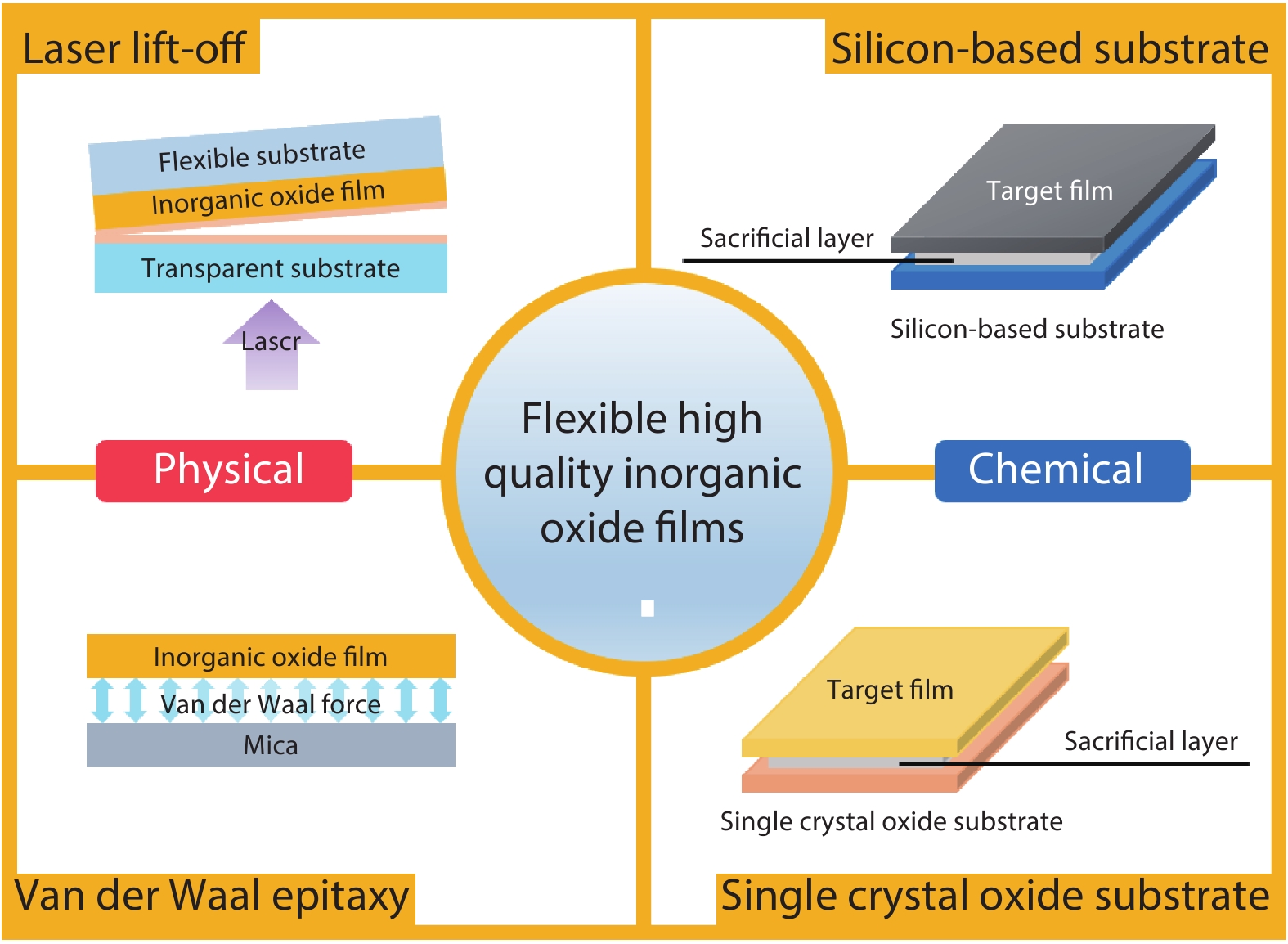
Fig. 1. (Color online) Advanced strategies for high quality inorganic oxide thin-film flexibility. In particular, the physical flexible strategies include LLO and van der Waal epitaxy, while the chemical flexible strategies include transferring films from silicon-based substrates and traditional single crystal oxide substrates to flexible substrates after etching the sacrificial layer.
![(Color online) Mechanical peeling through LLO. (a–d) Schematic illustrations of the LLO process in fabricating flexible memory, skin-like transistor, thermoelectric generator, NG[40, 41, 45, 46]. (e) Photograph of the flexible PZT thin film-based NG attached to a glass tube, and the inset shows the bent NG[46]. (f) X-ray diffraction results of PZT thin films on a flexible (top, red) PET and a sapphire (bottom, blue) substrate[46]. (g) The open-circuit voltage and cross-sectional current density measured from PZT thin film-based NG in the forward connections[46]. (h) The instantaneous lighting up of 105 blue LEDs in series when an NG device is unbent after slight bending, and the inset shows the driven LED arrays in a darkroom[46]. (i) Photograph of the frequency separator with iPANS, and the inset shows a single iPANS unit attached to a glass rod with a radius of curvature of 1.0 cm[47]. (j) The vibration displacement i) and vibration amplitude ii) information of the a-iPANS versus to sound wave with a frequency range of 100–1600 Hz[47].](/richHtml/jos/2020/41/4/041602/img_2.jpg)
Fig. 2. (Color online) Mechanical peeling through LLO. (a–d) Schematic illustrations of the LLO process in fabricating flexible memory, skin-like transistor, thermoelectric generator, NG[40 , 41 , 45 , 46 ]. (e) Photograph of the flexible PZT thin film-based NG attached to a glass tube, and the inset shows the bent NG[46 ]. (f) X-ray diffraction results of PZT thin films on a flexible (top, red) PET and a sapphire (bottom, blue) substrate[46 ]. (g) The open-circuit voltage and cross-sectional current density measured from PZT thin film-based NG in the forward connections[46 ]. (h) The instantaneous lighting up of 105 blue LEDs in series when an NG device is unbent after slight bending, and the inset shows the driven LED arrays in a darkroom[46 ]. (i) Photograph of the frequency separator with iPANS, and the inset shows a single iPANS unit attached to a glass rod with a radius of curvature of 1.0 cm[47 ]. (j) The vibration displacement i) and vibration amplitude ii) information of the a-iPANS versus to sound wave with a frequency range of 100–1600 Hz[47 ].
Fig. 3. (Color online) Mechanical peeling by van der Waal epitaxy on mica. (a) Schematic of deposition process for flexible CFO film monitored by RHEED in real time (left), and the magnetic hysteresis loops (right) show that the flexible CFO/mica exhibits solid magnetic properties regardless of bending[58 ]. (b) Crystal structure of the interface region between the CFO−BFO composite and mica substrate (left), and the M−H loops of BFO−CFO under bending conditions (right) are in agreement with the flexible CFO/mica[63 ]. (c) Optical images of bending mica/ SRO/BTCO (left) which shows great resistance switch characteristics (right)[64 ]. (d) MoO2/M-Mica can remain the resistance under different bending radii (right), and the whole MoO2 film can be removed from M-Mica (left)[29 ]. (e) Photo of mechanical peeling 10-μ m-thick mica (left) and P–E loops before and after the PZT film being bent to bending radius of 2.2 mm for 104 times[65 ]. (f) The flexible and transparent AZO/ Ag (8 nm)/AZO multilayer films (left) shows great resistivity (right) and transmittance even after annealing at 750 °C[72 ].
Fig. 4. (Color online) Transfer printing technology. (a) Schematic illustration of the generic process flow for transfer printing[77 ]. (b) Schematic diagrams of pick up (left) and printing (right) of a thin film[78 ]. (c) Schematic diagram of critical energy release rates for the film/substrate interface and for the stamp/film interface[78 ].
Fig. 5. (Color online) Transferring of oxide thin films grown on silicon-based substrates. (a–c) A cross sectional image (a), optical image (b) and dielectric properties (c) of the bendable PEO/Au/BTO/Pt/TiO2/SiO2/Si structure[80 ]. (d–f) Schematic illustration of etching SiO2 for flexible ITO/Si structure (d) and the measurement of the photodetector (e), and the barrier height of the bent ITO/Si heterojunction versus its bending radius (f) shows that the barrier height decreases with the bending radius[81 ]. (g–i) Schematic illustration of printing transfers the PZT nanoribbons to the pre-stretched PDMS (g), and the optical image and three-dimensional (3D) rendering of wavy PZT nanoribbon devices on PDMS (h), which the measured wavelength of wavy PZT nanoribbons as a function of applied tensile strain fits well with that of theory (i)[82 ]. (j) Schematic illustration of ion-sliced LNO exfoliation[83 ]. (k–m) SEM of the cross-section (k) and the transfer surface (l) of the LNO thin film, and the wavelength detuning with voltage as parameter of Si/LNO racetrack resonator (m)[83 ].
Fig. 6. (Color online) Flexible sensors based on VO2/PDMS structure. (a) The resistance versus temperature curves for the VO2 film in different states[85 ]. (b) Applied strain, relaxed strain and strain on VO2 at different slipping displacements[85 ]. (c) Strain on VO2 under heating and cooling cycles[85 ]. (d) The photograph of the breath sensor based on PI/VO2/PDMS structure[86 ]. (e) Response time and recovery time to breath[86 ]. (f) Resistance changes at different environment temperatures[86 ]. (g) Schematic illustration of electrical conductance of the sensor and the behavior of the disconnection-reconnection when applied strain on the x-axis (transverse) and y-axis (longitudinal)[87 ]. (h–j) Real-time monitoring signals (h), temperature signals (i) and pulse signals (j) of the flexible temperature-strain composite sensor[87 ].
Fig. 7. (Color online) Transferring oxide thin films grown on traditional oxide substrates. (a) Crystal structure of biaxial compression and stretching process during depositing films on substrate with a smaller or larger lattice[93 ]. (b) The strain induced by substrates as BFO films grown on different substrates[93 ]. (c) The magneto-optical effect of the same strain ETO grown on (110) DSO substrate, which proves that ETO becomes multiferroic under sufficient biaxial strain[93 ]. (d) Schematic illustration of transferring PZT by etching LSMO as a sacrificial layer[96 ]. (e) The I D–V G (top gate) characteristics of the ferroelectric PZT-gated transistor at V G (back gate) = 0[96 ]. (f) Schematic illustration of transfer processes of CFO thin films on flexible substrates[100 ]. (g, h) IP (g) and OPP (h) M−H hysteresis loops of the CFO thin films measured by vibrating sample magnetometer under different outward bending strains[100 ]. (i) Process schematic for heterostructure growth, oxide membrane release and transfer[102 ]. (j, k) IP magnetization loops of the SL (j) before and (k) after release[102 ].

Set citation alerts for the article
Please enter your email address
© Copyright 2018-2021 | Chinese Laser Press. All Rights Reserved 沪ICP备15018463号-20