
Tianyao Zhang, Guang Yao, Taisong Pan, Qingjian Lu, Yuan Lin. Flexible inorganic oxide thin-film electronics enabled by advanced strategies[J]. Journal of Semiconductors, 2020, 41(4): 041602
- Journal of Semiconductors
- Vol. 41, Issue 4, 041602 (2020)
Abstract
1. Introduction
Inorganic oxide thin films have attracted extensive attention thanks to their rich electrical, optical, thermal, mechanical, magnetic and other properties[
Benefiting from the rapid development of materials, mechanics and manufacturing science, flexible oxide thin films have been enabled to achieve various deformations, such as bending[
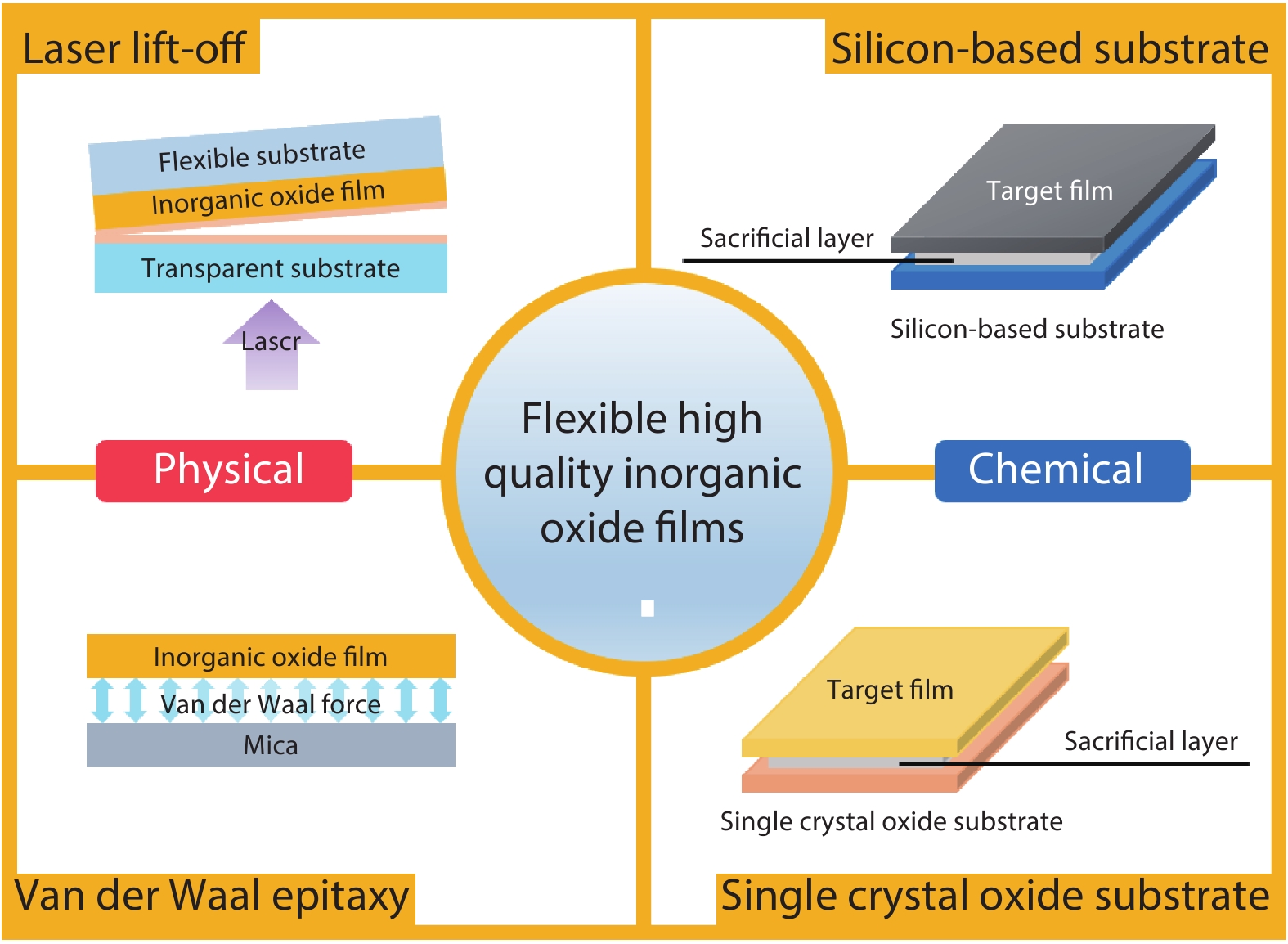
![]()
Figure 1.(Color online) Advanced strategies for high quality inorganic oxide thin-film flexibility. In particular, the physical flexible strategies include LLO and van der Waal epitaxy, while the chemical flexible strategies include transferring films from silicon-based substrates and traditional single crystal oxide substrates to flexible substrates after etching the sacrificial layer.
2. Physical strategies
Physical strategies refer to thin films that can be mechanically stripped to achieve macro-scale flexibility. LLO technique is a selective technology to remove one material from another[
2.1. Mechanical peeling through LLO
In the LLO technique, a transparent substrate is required to allow the laser beam to scan the entire interfacial film. Because the laser beam energy is lower than the band gap of substrate material and higher than that of upper film material, the laser beam energy can be absorbed only by the upper film, which results in damage-free separation of the upper film from the substrate[
![]()
Figure 2.(Color online) Mechanical peeling through LLO. (a–d) Schematic illustrations of the LLO process in fabricating flexible memory, skin-like transistor, thermoelectric generator, NG[
Lee’s group has fabricated flexible nanogenerator (NG) by growing the PbZr0.52Ti0.48O3 (PZT) film by sol-gel method with a subsequent crystallization step at 650 °C on sapphire substrate[
The LLO technique can realize the large area transfer of thin films with low damage. In addition, the substrate (such as sapphire used in LLO technique) can be reused[
2.2. Mechanical peeling by van der Waal epitaxy on mica
Micas are well-known phyllosilicates belonging to monoclinic structure. Muscovite (M-Mica) and fluorphlogopite (F-Mica) are common substrates in the thin film fabrication process. The M-Mica can be perfectly split along (001) plane by mechanical exfoliation, resulting in atomically smooth surface. M-Mica also possesses rich properties of chemical inertness, high transparency, and mechanical flexibility. The F-Mica has the similar properties to M-Mica, but it has lower flexibility than M-Mica, while its thermal stability is better than that of M-mica[
![]()
Figure 3.(Color online) Mechanical peeling by van der Waal epitaxy on mica. (a) Schematic of deposition process for flexible CFO film monitored by RHEED in real time (left), and the magnetic hysteresis loops (right) show that the flexible CFO/mica exhibits solid magnetic properties regardless of bending[
In the process of promoting device flexibility, the coupling between material properties and mechanical deformation should be of concern, including magnetostrictive properties, piezoelectric effects, and so on. Magnetostriction represents the relationship between the strain state and the magnetic state of a ferromagnet, which can be quantified by magnetostrictive coefficient (λ). To achieve higher response to magnetic field, Chu’s group has grown van der Waals epitaxial CoFe2O4 (CFO) thin films on M-Mica by the pulsed laser deposition (PLD) method. The reflective high energy electron diffraction (RHEED) is adopted to in situ monitor the deposition[
The clamping effect caused by rigid substrate has always been an important factor to weaken the magnetoelectric coupling. To overcome this problem, Chu’s group has prepared van der Waals epitaxy self-assembled BiFeO3 (BFO)-CFO bulk heterojunctions on M-Mica[
A flexible memory unit is an important part of flexible display screens and smart wearable devices. Although organic memory is more flexible than inorganic memory, it generally has poor high temperature stability and is easy to oxidize under illumination. Thus, it is important to develop inorganic memory with mechanical flexibility and high temperature stability. Chu’s group has grown van der Waals epitaxial PbZr0.2Ti0.8O3 thin films on M-Mica[
Transparent conducting oxides (TCO) have been widely used in solar cells, light emitting diodes, photodiodes, thin film transistors, photocatalysis, flat panel displays, gas sensors and energy-saving windows, and have become the basic components of advanced technology and equipment. With the development of portable and flexible electronic devices, it is particularly important to find a transparent and mechanically flexible base for TCO. As mentioned earlier, the commonly used transparent and flexible substrates are problematic; for example, ultra-thin glass is fragile and expensive, while polymer substrates such as PET and PI are not thermally stable, which impedes the growth of high-quality films. Meanwhile, micas are the ideal substrate for TCO preparation because of their high transparency, smooth atomic surface, thermal stability, chemical stability, flexibility, and mechanical durability. Chu’s group has grown van der Waals epitaxy TCO including ITO and Al-doped ZnO (AZO) films on M-Mica. A yttria-stabilized zirconia (YSZ) buffer layer was deposited before the ITO deposition, which is confirmed later that YSZ/mica heterostructure has good ionic conductivity and a high transmittance of more than 90% in the visible (380–800 nm) range[
In summary, micas can be widely used in various flexible devices. Generally, M-Mica has higher transparency, slightly better electrical properties and better flexibility than F-Mica, while F-Mica has better thermal stability than M-Mica, thus F-Mica is more suitable for the films which need higher annealing temperature for better crystallinity, and M-Mica is more suitable to increase the flexibility of films or devices. However, even though the advantages of micas enable the epitaxial layer to grow with its bulk lattice, it can hardly control the orientation of epitaxy layer, thus a thin buffer layer on the surface of mica or surface treatment for mica is usually needed[
3. Chemical strategies
For chemical strategies to make flexible thin film devices, the basic idea is transferring films from rigid substrates to flexible substrates after etching the sacrificial layer. In 2004, Rogers’s group first proposed microstructured silicon (μs-Si) technology, which involves photolithography, dry etching, wet etching and transfer printing process[
![]()
Figure 4.(Color online) Transfer printing technology. (a) Schematic illustration of the generic process flow for transfer printing[
Rogers’s group and Huang’s group have analyzed the dynamic control of the adhesive force of elastic stamps[
3.1. Transferring of oxide thin films grown on silicon-based substrates
Based on μs-SC technology, Lee’s group has deposited BTO films on prepared Pt/Ti/SiO2/Si substrate by radio frequency magnetron sputtering, following by annealing process above 600 °C[
![]()
Figure 5.(Color online) Transferring of oxide thin films grown on silicon-based substrates. (a–c) A cross sectional image (a), optical image (b) and dielectric properties (c) of the bendable PEO/Au/BTO/Pt/TiO2/SiO2/Si structure[
Metal–insulator transition (MIT) refers to the phenomenon of transforming or reversing from metal to insulator under certain external conditions, which has attracted considerable attention. Vanadium dioxide (VO2), as a well-known MIT material, will change from insulating monoclinic phase at low temperature to metal tetragonal phase at high temperature, and its optical and electrical properties will change dramatically at the same time. Its phase transition temperature (Tc) is close to room temperature and the resistance difference before and after phase transformation can reach 105. Moreover, VO2 has a high temperature coefficient of resistance (TCR) near room temperature, so it is very suitable for sensitive materials in temperature sensors. Lin’s group has prepared VO2 thin films on SiO2/Si substrates by the polymer-assisted deposition (PAD) method[
![]()
Figure 6.(Color online) Flexible sensors based on VO2/PDMS structure. (a) The resistance versus temperature curves for the VO2 film in different states[
Benefiting from the high TCR of VO2 near room temperature, Lin’s group has designed and fabricated a flexible breathing sensor with ultra-fast response based on PI/VO2/PDMS structure[
The transfer based on silicon-based substrates is compatible with the modern electronic industry. However, it is also obvious that epitaxial growth of most of the oxide thin films on silicon-based substrates is difficult because of the amorphous nature of the SiO2 layer. Therefore, it is very important to extend the transfer-printing technology used in silicon-based substrates to other single crystalline oxide substrates.
3.2. Transferring oxide thin films grown on single crystalline oxide substrates
With the development of strain engineering, researchers have done a lot of work on introducing large biaxial strain through heteroepitaxy. As shown in Fig. 7(a), following the energy preference of the substrate material or the lower layer epitaxial material, when the film material is deposited on the substrate with a larger lattice constant, the deposited atoms can cause the film to begin biaxial stretching. In contrast, when the film material is deposited on the substrate with a smaller lattice constant, the deposited atoms can cause the film to start biaxial compression[
![]()
Figure 7.(Color online) Transferring oxide thin films grown on traditional oxide substrates. (a) Crystal structure of biaxial compression and stretching process during depositing films on substrate with a smaller or larger lattice[
In recent years, many researchers have tried to transfer inorganic oxide films grown on single crystalline oxide substrates to other substrates using the approach of growing and etching a sacrificial layer. The sacrificial layers on single crystal oxide substrates correspond to the different etching solutions, which are often buffer solutions of different acids and salts[
After successfully transferring inorganic oxide films grown on single crystalline oxide substrates, researchers have found that the properties of inorganic oxide films can also be tailored with the stress regulation of flexibility, tension and torsion of inorganic oxide films transferred onto flexible substrates. Qi’s group has prepared PZT nanoribbons on MgO substrates[
Unlike etching with acid or acid salt solutions, Sr3Al2O6 (SAO) as sacrificial layer can be etched by water. Nie’s group has prepared free-standing BFO film with atomic layer thickness by etching the water-soluble SAO buffer layer, which opened the door of two-dimensional quantum phenomena with strong correlation[
Transferring the films grown on single crystalline oxide substrates broadens the application field of the transfer-printing technology, and develops strain engineering and the applications of oxide thin films at the same time. It is worth noting that the selection of sacrificial layers and the corresponding etching solutions play crucial roles in achieving flexible inorganic oxide thin films from the epitaxial layers on single crystalline oxide substrates.
4. Conclusion
Inorganic oxides have already occupied an important position in various applications because of their rich physical properties. By achieving the flexibility of inorganic oxides films, they also show great potential in wearable devices. At present, the main approaches to the flexibility of high quality inorganic oxide film can be divided into the physical approach of mechanical peeling films from rigid substrates, and the chemical approach of transferring films from rigid substrates to flexible substrates after etching the sacrificial layer. However, there are still many problems in the preparation of stable and high-performance inorganic oxide films. In particular, typical physical approaches may rely on LLO and van der Waal epitaxy on mica. In the LLO technique, the consumption of epitaxial layer and uneven heating or cooling of the upper layer during laser irradiation may affect the performance. Van der Waal epitaxy on mica is difficult to achieve films with good stretchability. For the chemical approach, after extending the flexible technologies used in silicon-based substrates to other single crystalline oxide substrates, the selections of sacrificial layers and corresponding etching solutions should also be broadened.
Flexible inorganic oxide films and devices have exhibited great performance, and they will play key roles in the next generation of flexible wearable devices. To meet the market’s requirements, the universality and practicability of methods for achieving flexible high quality inorganic oxide films should be further improved. Meanwhile, various flexible high quality inorganic oxide films should be integrated for practical applications. With the rapid development of materials, mechanics, manufacturing science and the rise of flexible devices, people are increasingly looking forward to the application of inorganic oxide functional films in flexible devices. This can not only greatly reduce the size of traditional devices, which will hopefully break Moore's law and greatly improve device performance, but can also expand the application field of flexible devices. At the same time, the development of inorganic oxides in rigid devices has matured and it is bound to accelerate with the development of flexible devices. Because the core of realizing inorganic oxide thin film flexible devices is to realize flexible inorganic oxide thin film, getting free-standing or self-supporting inorganic oxide thin film and realizing the integration of inorganic oxide thin film on flexible substrates have become the research focus. It is believed that flexible, high quality, inorganic oxide films and devices will promote the development of flexible wearable devices, and make our life more efficient and convenient in the electronic information era.
Acknowledgements
We acknowledge the financial support from the National Basic Research Program of China (973 Program) under Grant No. 2015CB351905, the Technology Innovative Research Team of Sichuan Province of China (No. 2015TD0005), "111" project (No. B13042), China National Funds for Distinguished Young Scientists (No. 61825102).
References
[1] K J Choi, M Biegalski, Y L Li et al. Enhancement of ferroelectricity in strained BaTiO3 thin films. Science, 306, 1005(2004).
[2] C Wang, X Ke, J Wang et al. Ferroelastic switching in a layered-perovskite thin film. Nat Commun, 7, 10636(2016).
[3] H Lan, F Liang, X Jiang et al. Pushing nonlinear optical oxides into the mid-infrared spectral region beyond 10
[4] Z Chen, Z Chen, C Y Kuo et al. Complex strain evolution of polar and magnetic order in multiferroic BiFeO3 thin films. Nat Commun, 9, 3764(2018).
[5] C Himcinschi, J Rix, C Röder et al. Ferroelastic domain identification in BiFeO3 crystals using Raman spectroscopy. Sci Rep, 9, 379(2019).
[6] Y Lin, D Y Feng, M Gao et al. Reducing dielectric loss in CaCu3Ti4O12 thin films by high-pressure oxygen annealing. J Mater Chem C, 3, 3438(2015).
[7] G Yao, M Gao, Y Ji et al. Surface step terrace tuned microstructures and dielectric properties of highly epitaxial CaCu3Ti4O12 thin films on vicinal LaAlO3 substrates. Sci Rep, 6, 34683(2016).
[8] G Yao, Y Ji, W Liang et al. Influence of vicinal surface on the anisotropic dielectric properties of highly epitaxial Ba0.7Sr0.3TiO3 thin films. Nanoscale, 9, 3068(2017).
[9] M C Choi, Y Kim, C S Ha. Polymers for flexible displays: from material selection to device applications. Prog Polym Sci, 33, 581(2008).
[10] J Jiang, Y Bitla, C W Huang et al. Flexible ferroelectric element based on van der Waals heteroepitaxy. Sci Adv, 3, e1700121(2017).
[11] J H Ahn, H S Kim, K J Lee et al. Heterogeneous three-dimensional electronics by use of printed semiconductor nanomaterials. Science, 314, 1754(2006).
[12] G Yao, D Jiang, J Li et al. Self-activated electrical stimulation for effective hair regeneration via a wearable omnidirectional pulse generator. ACS Nano, 13, 12345(2019).
[13] G Yao, L Kang, J Li et al. Effective weight control via an implanted self-powered vagus nerve stimulation device. Nat Commun, 9, 5349(2018).
[14] G Yao, H Zhang, S Zhang et al. Highly sensitive pressure switch sensors and enhanced near ultraviolet photodetectors based on 3D hybrid film of graphene sheets decorated with silver nanoparticles. RSC Adv, 7, 27281(2017).
[15] S Zhang, H Zhang, G Yao et al. Highly stretchable, sensitive, and flexible strain sensors based on silver nanoparticles/carbon nanotubes composites. J Alloys Compd, 652, 48(2015).
[16] D H Kim, J Song, W M Choi et al. Materials and noncoplanar mesh designs for integrated circuits with linear elastic responses to extreme mechanical deformations. Proc Natl Acad Sci USA, 105, 18675(2008).
[17] R H Kim, D H Kim, J Xiao et al. Waterproof AlInGaP optoelectronics on stretchable substrates with applications in biomedicine and robotics. Nat Mater, 9, 929(2010).
[18] D Y Khang, H Jiang, Y Huang et al. A stretchable form of single-crystal silicon for high-performance electronics on rubber substrates. Science, 311, 208(2006).
[19] H C Ko, G Shin, S Wang et al. Curvilinear electronics formed using silicon membrane circuits and elastomeric transfer elements. Small, 5, 2703(2009).
[20] A M V Mohan, N H Kim, Y Gu et al. Merging of thin- and thick-film fabrication technologies: toward soft stretchable “island-bridge” devices. Adv Mater Technol, 2, 1600284(2017).
[21] S Xu, Y Zhang, L Jia et al. Soft microfluidic assemblies of sensors, circuits, and radios for the skin. Science, 344, 70(2014).
[22] Z Huang, Y Hao, Y Li et al. Three-dimensional integrated stretchable electronics. Nat Electron, 1, 473(2018).
[23] K I Jang, K Li, H U Chung et al. Self-assembled three dimensional network designs for soft electronics. Nat Commun, 8, 15894(2017).
[24] W S Wong, T Sands, N W Cheung et al. Fabrication of thin-film InGaN light-emitting diode membranes by laser lift-off. Appl Phys Lett, 75, 1360(1999).
[25] T Fujii, A David, C Schwach et al. Micro cavity effect in GaN-based light-emitting diodes formed by laser lift-off and etch-back technique. Jpn J Appl Phys, 43, L411(2004).
[26] C F Chu, F I Lai, J T Chu et al. Study of GaN light-emitting diodes fabricated by laser lift-off technique. J Appl Phys, 95, 3916(2004).
[27] C I Li, J C Lin, H J Liu et al. Van der Waal epitaxy of flexible and transparent VO2 film on muscovite. Chem Mater, 28, 3914(2016).
[28] M I B Utama, M D L Mata, C Magen et al. Twinning-, polytypism-, and polarity-induced morphological modulation in nonplanar nanostructures with van der Waals epitaxy. Adv Funct Mater, 23, 1636(2013).
[29] C H Ma, J C Lin, H J Liu et al. Van der Waals epitaxy of functional MoO2 film on mica for flexible electronics. Appl Phys Lett, 108, 253104(2016).
[30] W S Wong, T Sands, N W Cheung et al. Damage-free separation of GaN thin films from sapphire substrates. Appl Phys Lett, 72, 599(1998).
[31] J Luo, R Pohl, L Qi et al. Printing functional 3D microdevices by laser-induced forward transfer. Small, 13, 1602553(2017).
[32] P Serra, A Piqué. Laser-induced forward transfer: fundamentals and applications. Adv Mater Technol, 4, 1800099(2018).
[33] J M Fernández-Pradas, P Sopeña, S González-Torres et al. Laser-induced forward transfer for printed electronics applications. Appl Phys A, 124, 214(2018).
[34] A Sorkio, L Koch, L Koivusalo et al. Human stem cell based corneal tissue mimicking structures using laser-assisted 3D bioprinting and functional bioinks. Biomaterials, 171, 57(2018).
[35] O Kérourédan, E Ribot, J Fricain et al. Magnetic resonance imaging for tracking cellular patterns obtained by laser-assisted bioprinting. Sci Rep, 8, 15777(2018).
[36] L Koch, O Brandt, A Deiwick et al. Laser-assisted bioprinting: a novel approach for bone regeneration application. Med Sci, 34, 125(2018).
[37] V Keriquel, H Oliveira, M Rémy et al. In situ printing of mesenchymal stromal cells, by laser-assisted bioprinting, for in vivo bone regeneration applications. Sci Rep, 7, 1778(2017).
[38] Y Gao, Y Li, R Li et al. An accurate thermomechanical model for laser-driven microtransfer printing. J Appl Mech-T ASME, 84, 064501(2017).
[39] H Luo, C Wang, C Linghu et al. Laser-driven programmable non-contact transfer printing of objects onto arbitrary receivers via an active elastomeric micro-structured stamp. Natl Sci Rev, 7, 296(2019).
[40] S Kim, J H Son, S H Lee et al. Flexible crossbar-structured resistive memory arrays on plastic substrates via inorganic-based laser lift-off. Adv Mater, 26, 7480(2014).
[41] H E Lee, S Kim, J Ko et al. Skin-like oxide thin-film transistors for transparent displays. Adv Funct Mater, 26, 6170(2016).
[42] Y F Cheung, K H Li, H W Choi et al. Flexible free-standing III-nitride thin films for emitters and displays. ACS Appl Mater Interfaces, 8, 21440(2016).
[43] T I Kim, Y H Jung, J Song et al. High-efficiency, microscale GaN light-emitting diodes and their thermal properties on unusual substrates. Small, 8, 1643(2012).
[44] H E Lee, J Choi, S H Lee et al. Monolithic flexible vertical GaN light-emitting diodes for a transparent wireless brain optical stimulator. Adv Mater, 30, e1800649(2018).
[45] S J Kim, H E Lee, H Choi et al. High-performance flexible thermoelectric power generator using laser multiscanning lift-off process. ACS Nano, 10, 10851(2016).
[46] K I Park, J H Son, G T Hwang et al. Highly-efficient, flexible piezoelectric PZT thin film nanogenerator on plastic substrates. Adv Mater, 26, 2514(2014).
[47] H S Lee, J Chung, G T Hwang et al. Flexible inorganic piezoelectric acoustic nanosensors for biomimetic artificial hair cells. Adv Funct Mater, 24, 6914(2014).
[48] M Mendes, J Fu, C Porneala et al. Lasers in the manufacturing of LEDs. Proc SPIE, 7584, 75840T(2010).
[49] S H Chuang, C T Pan, K C Shen et al. Thin film GaN LEDs using a patterned oxide sacrificial layer by chemical lift-off process. IEEE Photonics Technol Lett, 25, 2435(2013).
[50] A Morimoto, H Tanimura, H Yang et al. Platinum film patterning by laser lift-off using hydrocarbon film on insulating substrates. Appl Phys A, 79, 1015(2004).
[51] H Palneedi, J H Park, D Maurya et al. Laser irradiation of metal oxide films and nanostructures: applications and advances. Adv Mater, 30, e1705148(2018).
[52] X Xu, W Liu, Y Li et al. Flexible mica films for high-temperature energy storage. J Materiom, 4, 173(2018).
[53] S I Ohta. Synthetic mica and its applications. Clay Sci, 12, 119(2006).
[54] L Shen, M Liu, C Ma et al. Enhanced bending tuned magnetic properties in epitaxial cobalt ferrite nanopillar arrays on flexible substrate. Mater Horiz, 5, 230(2018).
[55] D Gao, Z Tan, Z Fan et al. All-inorganic flexible Ba0.67Sr0.33TiO3 thin films with excellent dielectric properties over a wide range of frequencies. ACS Appl Mater Interfaces, 11, 27088(2019).
[56] M F Tsai, J Jiang, P W Shao et al. Oxide heteroepitaxy based flexible ferroelectric transistor. ACS Appl Mater Interfaces, 11, 25882(2019).
[57] L T Quynh, C N Van, W Y Tzeng et al. Flexible heteroepitaxy photoelectrode for photo-electrochemical water splitting. ACS Appl Energy Mater, 1, 3900(2018).
[58] H J Liu, C K Wang, D Su et al. Flexible heteroepitaxy of CoFe2O4/muscovite bimorph with large magnetostriction. ACS Appl Mater Interfaces, 9, 7297(2017).
[59] P C Wu, P F Chen, T H Do et al. Heteroepitaxy of Fe3O4/muscovite: a new perspective for flexible spintronics. ACS Appl Mater Interfaces, 8, 33794(2016).
[60] W Hou, Z Zhou, L Zhang et al. Low-voltage-manipulating spin dynamics of flexible Fe3O4 films through ionic gel gating for wearable devices. ACS Appl Mater Interfaces, 11, 21727(2019).
[61] W Liu, R Ma, M Liu et al. Highly stable in-plane microwave magnetism in flexible Li0.35Zn0.3Fe2.35O4 (111) epitaxial thin films for wearable devices. ACS Appl Mater Interfaces, 10, 32331(2018).
[62] W Liu, M Liu, R Ma et al. Mechanical strain-tunable microwave magnetism in flexible CuFe2O4 epitaxial thin film for wearable sensors. Adv Funct Mater, 28, 1705928(2018).
[63] T Amrillah, Y Bitla, K Shin et al. Flexible multiferroic bulk heterojunction with giant magnetoelectric coupling via the van der Waals epitaxy. ACS Nano, 11, 6122(2017).
[64] Y Yang, G Yuan, Z Yan et al. Flexible, semitransparent, and inorganic resistive memory based on BaTi0.95Co0.05O3 film. Adv Mater, 29, 1700425(2017).
[65] W Gao, L You, Y Wang et al. Flexible PbZr0.52Ti0.48O3 capacitors with giant piezoelectric response and dielectric tunability. Adv Electron Mater, 3, 1600542(2017).
[66] Z Liang, C Ma, L Shen et al. Flexible lead-free oxide film capacitors with ultrahigh energy storage performances in extremely wide operating temperature. Nano Energy, 57, 519(2019).
[67] Z Liang, M Liu, L Shen et al. All-inorganic flexible embedded thin film capacitors for dielectric energy storage with high performance. ACS Appl Mater Interfaces, 11, 5247(2019).
[68] J Wu, Z Liang, C Ma et al. Flexible lead-free BaTiO3 ferroelectric elements with high performance. IEEE Electron Device Lett, 40, 889(2019).
[69] P C Wu, Y P Lin, Y H Juan et al. Epitaxial yttria-stabilized zirconia on muscovite for flexible transparent ionic conductors. ACS Appl Nano Mater, 1, 6890(2018).
[70] Y Bitla, C Chen, H C Lee et al. Oxide heteroepitaxy for flexible optoelectronics. ACS Appl Mater Interfaces, 8, 32401(2016).
[71] S Ke, C Chen, N Fu et al. Transparent indium tin oxide electrodes on muscovite mica for high-temperature-processed flexible optoelectronic devices. ACS Appl Mater Interfaces, 8, 28406(2016).
[72] M Li, Y Wang, Y Wang et al. AZO/Ag/AZO transparent flexible electrodes on mica substrates for high temperature application. Ceram Int, 43, 15442(2017).
[73] Y Yang, W Gao, Z Xie et al. An all-inorganic, transparent, flexible, and nonvolatile resistive memory. Adv Electron Mater, 4, 1800412(2018).
[74] Y Zhang, Y Cao, H Hu et al. Flexible metal-insulator transitions based on van der Waals oxide heterostructures. ACS Appl Mater Interfaces, 11, 8284(2019).
[75] E Menard, K J Lee, D Y Khang et al. A printable form of silicon for high performance thin film transistors on plastic substrates. Appl Phys Lett, 84, 5398(2004).
[76] K J Lee, J J Lee, H Hwang et al. A printable form of single-crystalline gallium nitride for flexible optoelectronic systems. Small, 1, 1164(2005).
[77] M A Meitl, Z T Zhu, V Kumar et al. Transfer printing by kinetic control of adhesion to an elastomeric stamp. Nat Mater, 5, 33(2005).
[78] X Feng, M A Meitl, A M Bowen et al. Competing fracture in kinetically controlled transfer printing. Langmuir, 23, 12555(2007).
[79] Z Yan, T Pan, M Xue et al. Thermal release transfer printing for stretchable conformal bioelectronics. Adv Sci, 4, 1700251(2017).
[80] K I Park, S Y Lee, S Kim et al. Bendable and transparent barium titanate capacitors on plastic substrates for high performance flexible ferroelectric devices. Electrochem Solid State Lett, 13, G57(2010).
[81] G Yao, T Pan, Z Yan et al. Tailoring the energy band in flexible photodetector based on transferred ITO/Si heterojunction via interface engineering. Nanoscale, 10, 3893(2018).
[82] X Feng, B D Yang, Y Liu et al. Stretchable ferroelectric nanoribbons with wavy configurations on elastomeric substrates. ACS Nano, 5, 3326(2011).
[83] L Chen, J Nagy, R M M Reano et al. Patterned ion-sliced lithium niobate for hybrid photonic integration on silicon. Opt Mater Express, 6, 2460(2016).
[84] W Liang, M Gao, C Lu et al. Enhanced metal-insulator transition performance in scalable vanadium dioxide thin films prepared using a moisture-assisted chemical solution approach. ACS Appl Mater Interfaces, 10, 8341(2018).
[85] F Liao, Z Yan, W Liang et al. Tuning the metal-insulator transition of vanadium dioxide thin films using a stretchable structure. J Alloys Compd, 705, 468(2017).
[86] F Liao, Z Zhu, Z Yan et al. Ultrafast response flexible breath sensor based on vanadium dioxide. J Breath Res, 11, 036002(2017).
[87] F Liao, C Lu, G Yao et al. Ultrasensitive flexible temperature-mechanical dual-parameter sensor based on vanadium dioxide films. IEEE Electron Device Lett, 38, 1128(2017).
[88] M Gao, Z Qi, C Lu et al. Interplay between extra charge injection and lattice evolution in VO2/CH3NH3PbI3 heterostructure. Phys Status Solidi RRL, 12, 1700416(2018).
[89] Z Kang, M Gao, C Lu et al. Thickness-modulated temperature dependent optical properties of VO2 thin films. Appl Phys A, 125, 63(2019).
[90] C Lu, W Liang, G G Min et al. Terahertz transmittance of cobalt-doped VO2 thin film: investigated by terahertz spectroscopy and effective medium theory. IEEE Trans THz Sci Technol, 9, 177(2019).
[91] W Liang, o Z Zhuo, Y Ji et al. In-plane orientation-dependent metal-insulator transition in vanadium dioxide induced by sublattice strain engineering. npj Quantum Mater, 4, 39(2019).
[92] P Fratzl, F G Barth. Biomaterial systems for mechanosensing and actuation. Nature, 462, 442(2009).
[93] D G Schlom, L Q Chen, C J Fennie et al. Elastic strain engineering of ferroic oxides. MRS Bull, 39, 118(2014).
[94] A Chen, Q Su, H Han et al. Metal oxide nanocomposites: a perspective from strain, defect, and interface. Adv Mater, 31, 1803241(2018).
[95] G Bridoux, J Barzola-Quiquia, F Bern et al. An alternative route towards micro- and nano-patterning of oxide films. Nanotechnology, 23, 085302(2012).
[96] S R Bakaul, C R Serrao, M Lee et al. Single crystal functional oxides on silicon. Nat Commun, 7, 10547(2016).
[97] L Shen, L Wu, Q Sheng et al. Epitaxial lift-off of centimeter-scaled spinel ferrite oxide thin films for flexible electronics. Adv Mater, 29, 1702411(2017).
[98] Y Qi, N T Jafferis, K Lyons et al. Piezoelectric ribbons printed onto rubber for flexible energy conversion. Nano Lett, 10, 524(2010).
[99] Y Qi, J Kim, T D Nguyen et al. Enhanced piezoelectricity and stretchability in energy harvesting devices fabricated from buckled PZT ribbons. Nano Lett, 11, 1331(2011).
[100] Y Zhang, L Shen, M Liu et al. Flexible quasi-two-dimensional CoFe2O4 epitaxial thin films for continuous strain tuning of magnetic properties. ACS Nano, 11, 8002(2017).
[101] D Ji, S Cai, T R Paudel et al. Freestanding crystalline oxide perovskites down to the monolayer limit. Nature, 570, 87(2019).
[102] D Lu, D J Baek, S S Hong et al. Synthesis of freestanding single-crystal perovskite films and heterostructures by etching of sacrificial water-soluble layers. Nat Mater, 15, 1255(2016).
[103] H Wang, L Shen, T Duan et al. Integration of both invariable and tunable microwave magnetisms in a single flexible La0.67Sr0.33MnO3 thin film. ACS Appl Mater Interfaces, 11, 22677(2019).
[104] G Dong, S Li, M Yao et al. Super-elastic ferroelectric single-crystal membrane with continuous electric dipole rotation. Science, 366, 475(2019).

Set citation alerts for the article
Please enter your email address
© Copyright 2018-2021 | Chinese Laser Press. All Rights Reserved 沪ICP备15018463号-20