
Yu Yu, Yating Zhang, Lufan Jin, Zhiliang Chen, Yifan Li, Qingyan Li, Mingxuan Cao, Yongli Che, Haitao Dai, Junbo Yang, Jianquan Yao, "Self-powered lead-free quantum dot plasmonic phototransistor with multi-wavelength response," Photonics Res. 7, 149 (2019)
- Photonics Research
- Vol. 7, Issue 2, 149 (2019)
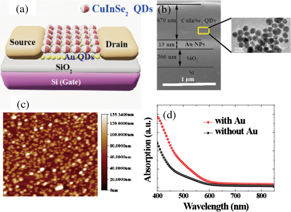
Fig. 1. (a) Schematic diagram of plasmonic CuInSe 2 CuInSe 2 CuInSe 2 CuInSe 2
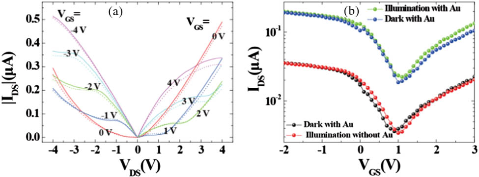
Fig. 2. Photoelectronic properties of the device. (a) Output characteristics (I DS − V DS V GS 700 mW · cm − 2 CuInSe 2 845 mW · cm − 2 845 mW · cm − 2 V DS = 1.2 V
Fig. 3. Time-dependent response of the device at zero bias with different wavelengths and irradiation intensities. (a), (d) 405 nm; (b), (e) 532 nm; (c), (f) 808 nm.
Fig. 4. Photoresponsivity (R
Fig. 5. Time-dependent response of the device with or without deposited Au NPs as a function of irradiance under different wavelengths with chopper frequency of 3944 Hz at a bias of 0 V: (a) 405 nm, (b) 532 nm, and (c) 808 nm.
Fig. 6. (a) Structure diagram of FDTD simulation. The field distributions in the x–y plane under (b) 405 nm, (c) 532 nm, and (d) 808 nm light illumination.
Fig. 7. Electronic band structure and working principle of the CuInSe 2
|
Table 1. Comparison in Device Performance of CuInSe 2


Set citation alerts for the article
Please enter your email address

© Copyright 2018-2021 | Chinese Laser Press. All Rights Reserved 沪ICP备15018463号-20