Abstract
Because they possess excellent visible light absorption properties, lead-free colloidal copper-based chalcogenide quantum dots (QDs) have emerged in photoelectronic fields. By means of localized surface plasmonic resonance (LSPR), the absorption properties of QDs can be enhanced. In this paper, we fabricate a lead-free QD field effect phototransistor (FEpT) by utilizing the LSPR enhancement of Au nanoparticles (NPs). The plasmonic FEpT demonstrates responsivity up to and a specific detectivity of Jones at zero bias under illumination by a 532 nm laser, values that are enhanced by approximately 200% more than devices without Au NPs. Particularly, the FEpT exhibits a multi-wavelength response, which is photoresponsive to 405, 532, and 808 nm irradiations, and presents stability and reproducibility in the progress of ON–OFF cycles. Furthermore, the enhancement induced by Au NP LSPR can be interpreted by finite-difference time domain simulations. The low-cost solution-based process and excellent device performance strongly underscore lead-free QDs as a promising material for self-powered photoelectronic applications, which can be further enhanced by Au NP LSPR.1. INTRODUCTION
Self-powered photodetectors have advantages that include low power consumption, energy savings, and passive detection without any external power sources [1–4]. Unfortunately, traditional self-powered photodetectors made by Si, SiC, and InP still suffer from low responsivity [5]. By contrast, new types of functional nanomaterials can solve this problem owing to strong light absorption [6], particularly for colloidal quantum dots (CQDs).
CQDs have applications in a wide range of solution-processed photoelectronic devices, including solar cells [7–9], light-emitting diodes [10,11], infrared imaging [12], and photodetectors [13–16]. Particularly, quantum dot photodetectors (QDPDs) have focused largely on the utilization of IV−VI (PbS, PbSe) quantum dots (QDs) due to their near-infrared conduction band edge values and established synthetic procedures. However, the presence of Pb cations generally limits their application.
As one of the lead-free QDs, colloidal copper-based chalcogenide (, and Se) QDs are attractive in a broad range of applications, specifically photovoltaics [17–21], photobiological labels [22–26], light-emitting devices [27–29], electrocatalysts [30,31], and photodetectors [32], due to their lower toxicity, better biocompatibility, and unique photoelectric properties [33]. Particularly, by exhibiting a tunable bandgap ranging from 0.96 to 1.65 eV [21], QDs have a higher optical absorption coefficient in the visible spectral range [17,21]. Therefore, they are considered more promising candidates for use in photodetection devices.
Sign up for Photonics Research TOC. Get the latest issue of Photonics Research delivered right to you!Sign up now
As we all know, metal plasma can be implemented to increase light absorbance and reduce recombination during charge transport to current collectors [33–36]; thus, it can improve the photoelectronic properties. As for CQDs, the localized surface plasmonic resonance (LSPR) effect has been utilized to increase photoelectric properties by coupling with incident light in many photodetectors [37–40]. For instance, Dong et al. [40] demonstrated a QD photodetector overlapping with LSPR, which exhibited higher light ON–OFF and photocurrent than nonplasmonic QDs. Chang et al. [37] reported InAs CQD photodetectors enhanced by LSPR, demonstrating a 130% enhancement of photoresponse and detectivity. To our knowledge, field effect phototransistors (FEpTs) based on QDs enhanced by LSPR have never been studied.
In this paper, plasmonic lead-free FEpTs are fabricated by deposition of Au nanoparticles (NPs) for multi-wavelength detection. Particularly, light signals can be efficiently converted into electrical signals at zero volt bias. Meanwhile, the device demonstrates responsivity up to 2.7 μA/W, and detectivity of Jones. The plasmonic FEpT exhibits fast response (a rise time of 0.1 ms and a decay time of 0.06 ms), and excellent stability and reproducibility. Moreover, with the effect of Au NP LSPR for the device, the photocurrent is enhanced by approximately 200%. The enhancement mechanism is attributed to the coupling effect between QDs and Au NPs, which is confirmed by theoretical simulation through the finite-difference time domain (FDTD) method. Therefore, superior detection performance by the enhancement of the Au NP plasmonic effect promises great potential for future optoelectronic devices.
2. DEVICE STRUCTURE AND FABRICATION
The plasmonic QDs FEpT was fabricated by the following process. First, the substrate was prepared by a highly doped n-type silica wafer ( Si), and a silica dioxide () layer with thickness of 300 nm was thermally grown on the substrate. Sequentially, the substrate was cleaned by ultrasonic treatment in acetone, alcohol, and deionized water for 15 min. Second, Au NPs (purchased from Nanjing Muke Company) were deposited on the with a self-assembly method. In detail, Au NP solution added by pipette was deposited on the substrate by spin-coating at 6000 r/min for 60 s. Third, the lead-free QDs film was deposited at 3000 r/min for 60 s. Finally, utilizing a sophisticated shadow mask, drain and source electrodes were thermally evaporated at a rate of () at pressure of . Each device was dried for 24 h in vacuum conditions before further measurements. All the measurements were performed in air at room temperature.
3. RESULTS AND DISCUSSION
Figure 1(a) depicts the schematic diagram of the plasmonic QDs FEpT. For the bottom-gate configuration, a highly doped n-type silicon wafer ( Si) covered with a 300 nm thick layer (capacitance of ) was used as the gate electrode. Then, the substrate was cleaned by ultrasonic treatment in propanol, acetone, and deionized water for 10 min each. After that, the charge trapping layer of 13 nm thick Au NPs [shown in the sectional scanning electron microscope (SEM) image in Fig. 1(b)] was transferred onto the substrate by the self-assembly method. Meanwhile, the transmission electron microscopy (TEM) image in the inset of Fig. 1(b) depicts the nearly monodisperse spherical shape of QDs [41]. The coverage of the Au NP layer configuration on the substrate was measured by atomic force microscopy (AFM). Figure 1(c) depicts a topography image working at trapping mode, which exhibits good homogeneous surface morphologies. Next, colloidal QDs made by the hydrothermal synthesis method were spin-coated on the device with rotating speed of 3000 r/min. Finally, the source and drain electrodes of Cr/Au were deposited through a thermal evaporation method assisted by a shadow mask [42], where the channel length () and channel width () were defined as 0.1 mm and 2.5 mm, respectively. Notably, the thickness of the photosensitive layer is a key parameter for FEpTs, given the abilities of either light absorption or gate electrode modulation. Specifically, if the active layer is too thin, it cannot absorb sufficient light to convert photoexcitons. In addition, pinholes in the thin QD film will cause inhomogeneous conduction in the channel, while if the film is too thick, the bottom gate will modulate the channel ineffectively. After optimization, the thickness of the QD film prepared in the phototransistors is fixed at [shown in Fig. 1(b)]. The absorption properties of QD film with deposited Au NPs (red line) or not (black line), are depicted in Fig. 1(d). This indicates that the absorption properties can be enhanced by considering the Au NP LSPR. For measurement details, the source (with ground connection) and drain electrodes were connected with a Keithley 2400, the channel current flowing into the drain electrode () was also measured by a source meter of Keithley 2400, and the gate voltage () was applied by a DC voltage source of HP6030A. Photoelectrical measurements were also performed based on this system under illumination by 405, 532, and 808 nm lasers.
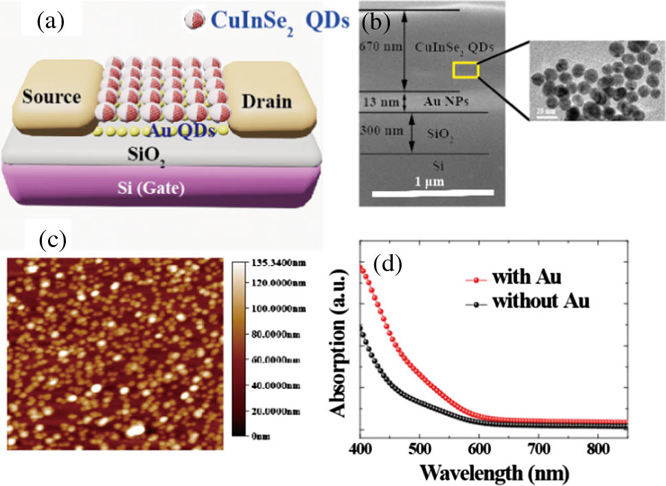
Figure 1.(a) Schematic diagram of plasmonic QD FEpT architecture. (b) Cross-sectional SEM image of composite film between and Au NPs (inset: TEM image of pristine QDs). (c) AFM image of Au NPs on silicon substrate. (d) Optical absorption spectra of QDs with (red line) and without (black line) deposited Au NPs on glass substrate.
To characterize the electronic properties of plasmonic QDs FEpTs, output characteristics of pristine QD FEpTs (in darkness, dashed lines; under illumination of with a 405 nm laser, solid lines) with different gate voltages (0, , , , ) are depicted in Fig. 2(a). The device exhibits typically ambipolar characteristics. To look further into the modulation of gate voltage, Fig. 2(b) depicts the transfer characteristics of typical FEpTs, with Au NP deposition (black line, in darkness; red line, under illumination of by an 808 nm laser) and without Au NP deposition (blue line, in darkness; green line, under illumination of by an 808 nm laser) under bias voltage . Each device exhibits typically ambipolar characteristics, and the “V” shape of the transfer curves is particularly presented, manifesting either electron or hole transport in the n-type or p-type channels of the device, respectively. Particularly, for the plasmonic FEpT, the mechanism can be interpreted as that after the two materials contact each other, owing to the existence of accepter states in Au NPs, electrons are injected into these states [40]. The effective electric field determines the flowing direction and an amount of the electrons separated from photoexcitons tends to reside in the Au NP layer [43]. Therefore, the shift of minimum V-shaped transfer curve toward negative [the red line shown in Fig. 2(b)] can be ascribed to the efficient photoexciton separation and hole transfer at the interface [44]. Comparing with the condition without irradiation, the values of become larger. It can be understood that the photo-induced carriers can be generated under the condition of light irradiation. Therefore, the enhancements of are ascribed to the increase of the electron and hole concentrations [42]. Meanwhile, after considering the LSPR effect, the drain–source dark current in the plasmonic FEpT can be suppressed, and the shift is more significantly observed as the gate bias varies [40]. This is because more electrons are trapped in the surface of Au NPs, leading to a large width of the conducting channel [40]. Therefore, the bottom gate will effectively modulate the channel.

Figure 2.Photoelectronic properties of the device. (a) Output characteristics ( curves) under different (1 V increment) of plasmonic FEpT (dashed lines, in darkness; solid lines, under illumination of of a 405 nm laser). (b) Transfer characteristics of typical FEpTs, after Au NP deposition (black line, in darkness; red line, under illumination of an of 808 nm laser) and before Au NPs deposition (blue line, in darkness; green line, under illumination of of an 808 nm laser) with applied bias voltage .
Corresponding to Fig. 1(d), QDs exhibit broad absorption ranging from 400 to 850 nm. Illuminated by light with different wavelengths (405, 532, and 808 nm), photoswitching curves of the device are presented in Figs. 3(a)–3(c) under periodic illumination intensity of . The device exhibits stable and excellent reproducibility in each illumination. Meanwhile, the photocurrents excited by 405, 532, and 808 nm are about 120, 100, and 60 nA, respectively. Physically, this indicates that the incident photo energy must be larger than the energy gap; in other words, photocurrent generation needs to match the basic condition. Only these incident photons with enough photon energy can excite electrons from the valence band maximum to the conduction band minimum (CBM), generating the photocurrent. Therefore, more electrons and photoexcitons can be excited with stronger incident photo energy light at the short wavelength and contribute more to photocurrent. Under the irradiation of stronger energy light at the shorter wavelength, it leads to a huge enhancement in the density of free carriers, which in turn results in easier carrier transport and tunneling, and thus to greatly enhanced photocurrents. Figures 3(d)–3(e) depict the drain–source currents () versus illumination irradiance () under different wavelengths, in which photocurrent increases linearly with at low irradiance, then tends to saturate at high irradiance. It is concluded that with larger irradiance, more photoexcitons can be excited, leading to lower built-in potential of the Schottky barrier and a higher probability to pass over the Schottky barrier. If the electrons pass over the Schottky barrier, then photocurrent will increase linearly in the progress of the carrier flowing to the external circuit. Note that, with irradiance continuing to increase, the quantity of photoexcitons is no longer increased in QDs, and thus they cannot be converted to photocurrent, leading to saturation of the photocurrent. To further investigate the photo properties of the device, as a vital parameter, photoresponsivity () is calculated by [45–47] where and represent the drain current under illumination and in darkness. , , and are power density, irradiance, and the effective channel area, respectively. The photoresponsivities of the plasmonic QDs FEpT as a function of irradiance under different wavelengths are shown in Fig. 4. Particularly, the maximum photoresponsivity () is calculated to be 2.7 μA/W at irradiance of under the illumination of a 532 nm laser. Other key parameters characterizing photodetector performance, such as detectivity (), noise equivalent power (NEP), and gain () can be given as [48] , , and , respectively, where is the responsivity, is the area of the detector, is the charge of an electron, and is the dark current. The , NEP, and of the device are Jones, , and , respectively. Responsivities in plasmonic QDs FEpT under illumination of 405 nm exhibit a first increasing then decreasing trend. However, it decreases with the increasing irradiance in particular at wavelengths of 532 and 808 nm. This is attributed to the existence of acceptor states in Au NPs. To demonstrate in detail, we construct a measurement system referring to Ref. [49]. Meanwhile, as another key parameter for photodetectors, photoresponse speed determines the capability of a photodetector to follow a fast-switching optical signal. It also reflects a series of times during the whole transition progress in which it concludes the vital acceptor progress. To highlight this progress of the device, initially we adopt a pump laser with different light irradiance at each wavelength, varying the chopper frequency. Figure 5 shows the time-dependent drain current response of the device with the maximum light irradiance under [Fig. 5(a)] 405 nm, [Fig. 5(b)] 532 nm, and [Fig. 5(c)] 808 nm, with maximum chopper frequency of 3944 Hz. The drain current quickly increases as soon as the light switch is turned on and then decreases when the light switch is turned off. This indicates that the increased charge intensity lowers the effective barrier height upon illumination, which allows easier charge tunneling and transportation than that of the device in darkness. Particularly, the red dashed circles denote the progress of photo-induced electrons excited to the acceptor states in an Au nanoparticle. Furthermore, the amplitude of this progress decreases with the enhancement of wavelength. This indicates that more electrons and photoexcitons can be excited with larger incident photo energy light at the short wavelength and contribute more to photocurrent. This also indicates that electrons have to overcome the Schottky barrier during transport [50]. Under the illumination of larger energy light at the shorter wavelength, the built-in potential of the Schottky barrier decreases, resulting in a large increase in the free carrier density, leading to easier carrier transport and tunneling and thus to greatly enhanced photocurrents. Furthermore, the device exhibits photoresponse for a fluorescent lamp, indicating that our device has a strong light detection property for weak illumination.
Figure 3.Time-dependent response of the device at zero bias with different wavelengths and irradiation intensities. (a), (d) 405 nm; (b), (e) 532 nm; (c), (f) 808 nm.
Figure 4.Photoresponsivity () of the device with or without deposited Au NPs as a function of irradiance under different wavelengths with chopper frequency of 3944 Hz at a bias of 0 V: (a) 405 nm, (b) 532 nm, and (c) 808 nm.
To validate the experimental results, the software FDTD Solutions is utilized to better demonstrate the enhancement by effects of Au LSPR on QD photogenerated carriers. Figure 6(a) presents the simulation schematics of the plasmonic device. The electric field distribution in the vicinity of Au NPs is calculated by FDTD simulation. In concordance with experimental results, particularly in the SEM and TEM images, we assume that the 13 nm diameter Au NPs are packed in the x–y plane under the compact QD film in thickness of 670 nm [shown in Fig. 1(b)]. The incident light illuminates toward the top surface with propagating direction of –z. Figures 6(b)–6(d) show the field distributions in the x–y plane of a single Au NP deposited in the QDs film under light illumination with the wavelengths of 405 nm [Fig. 6(b)], 532 nm [Fig. 6(c)], and 808 nm [Fig. 6(d)]. Obviously, the enhancement of the electric field in the vicinity of the Au NPs can be observed after packing under the QD film. The degree of electric field distribution is indicated by the shading in red or blue. Particularly, as described in each map of Figs. 6(b)–6(d), the distributions of the strongest and weakest enhancement are represented by the dark red and dark blue, respectively. Compared with different distributions with LSPR enhancement for QDs, the enhancement degree under the wavelength of 405 nm [shown in Fig. 6(b)] is the strongest (approaching times). This indicates that under the illumination of shorter wavelength light with larger energy, the photogenerated carrier density will have a large increase, so as to enhance photocurrents for the device. Therefore, the theoretical simulation is consistent with the experimental results.
In addition, as another parameter characterizing the properties of the photodetector, temporal photocurrent responses of the device with (solid lines) or without (dashed lines) Au LSPR under different wavelengths are shown in Fig. 5. The rise and decay times in the devices with Au NPs LSPR effect and without Au NPs are approximately 0.1 ms/0.06 ms and 0.05 ms/0.03 ms, respectively. This is attributed to the additional progress during photogenerated carriers trapped in the acceptor states. Recently, using pristine , Guo et al. [41] reported switching times of FEpTs of and 150 ms. To compare characteristics without the Au NP LSPR effect, several key parameters are listed in Table 1.
Figure 5.Time-dependent response of the device with or without deposited Au NPs as a function of irradiance under different wavelengths with chopper frequency of 3944 Hz at a bias of 0 V: (a) 405 nm, (b) 532 nm, and (c) 808 nm.
Figure 6.(a) Structure diagram of FDTD simulation. The field distributions in the x–y plane under (b) 405 nm, (c) 532 nm, and (d) 808 nm light illumination.
| Device | Idark [nA] | Iillu [nA] | Idark/Iillu | Responsivity [μA·W−1] | D* [103 Jones] | Rise/Decay Time [ms] |
| Without Au NPs | 8.2 | 13.8 | 1.6 | 2.0 | 7.0 | 0.05/0.03 |
| With Au NPs | 5.7 | 28.9 | 5.0 | 4.4 | 14.4 | 0.1/0.06 |
Table 1. Comparison in Device Performance of FEpTs with or without Au NPs at the Strongest Enhancement with Wavelength of 405 nm
The sensing mechanism of plasmonic FEpTs is schematically described in Fig. 7. According to band theory, electron–hole pairs (photoexcitons) are generated when the incident photon energy is greater than the bandgap of QDs. Then, electrons and holes are separated from photoexcitons by applying external bias, generating the photocurrent. Under continuous illumination, electrons can transport to the interface acceptor states in Au NPs. The conduction electrons are trapped at the acceptor states of Au NPs. Owing to the acceptor states during illumination, the conductivity also continuously decreases until the acceptor states are completely filled. Given short wavelength light with larger photon energy, more photogenerated electrons can be excited. Therefore, the amplitude at short wavelength varies significantly. Particularly, electrons can be excited into higher energy level of QDs illuminated by pump light with larger photon energy [shorter wavelength, 405 nm, shown in Fig. 5(a)], leading to the increase of photocurrent. The acceptor states in Au NPs are located between the high energy level and CBM in QDs. Therefore, the electrons in the higher energy level will energetically be transited into the acceptor states. After completion of filling to saturation, electrons in the saturated acceptor states will jump to the CBM in the QDs, leading to continued increase in the photocurrent. However, in darkness, vacancies will occur in saturated acceptor states and can be filled with electrons from the high energy level in QDs, leading to the decrease of photocurrent.
Figure 7.Electronic band structure and working principle of the QD FEpTs with Au NPs.
4. CONCLUSION
In summary, plasmonic lead-free quantum dot (QD) field effect phototransistors (FEpTs) were fabricated through a low-cost, solution-processed strategy. The FEpTs exhibit self-powered multi-wavelength response, particularly, for 405, 532, and 808 nm irradiations. It is worth mentioning that the relevant properties can be enhanced after considering the Au NP localized surface plasmonic resonance (LSPR) effect. Meanwhile, this enhancement has been revealed by the finite-difference time domain (FDTD) method. Furthermore, for photoelectronic properties in the plasmonic device, the responsivity and the detectivity are up to and Jones, respectively. The plasmonic device presents stability and reproducibility in the progress of ON–OFF cycles, and fast rise and decay times of the photocurrent are and . Therefore, the low-cost solution-based process and excellent device performance strongly underscore lead-free QDs as a promising material for self-powered photoelectronic applications, which can be further enhanced by the Au NP plasmonic effect.
References
[1] J. Feng, M. Graf, K. Liu, D. Ovchinnikov, D. Dumcenco, M. Heiranian, V. Nandigana, N. R. Aluru, A. Kis, A. Radenovic. Single-layer MoS2 nanopores as nanopower generators. Nature, 536, 197-200(2016).
[2] S. Xu, Y. Qin, C. Xu, Y. Wei, R. Yang, Z. L. Wang. Self-powered nanowire devices. Nat. Nanotechnol., 5, 366-373(2010).
[3] F. Zhang, Y. Zang, D. Huang, C. A. Di, D. Zhu. Flexible and self-powered temperature-pressure dual-parameter sensors using microstructure-frame-supported organic thermoelectric materials. Nat. Commun., 6, 8356(2015).
[4] Z. Wang, R. Yu, C. Pan, Z. Li, J. Yang, F. Yi, Z. L. Wang. Light-induced pyroelectric effect as an effective approach for ultrafast ultraviolet nanosensing. Nat. Commun., 6, 8401(2015).
[5] S. F. Leung, K. T. Ho, P. K. Kung, V. K. S. Hsiao, H. N. Alshareef, Z. L. Wang, J. H. He. A self-powered and flexible organometallic halide perovskite photodetector with very high detectivity. Adv. Mater., 30, 1704611(2018).
[6] C. R. Kagan, E. Lifshitz, E. H. Sargent, D. V. Talapin. Building devices from colloidal quantum dots. Science, 353, aac5523(2016).
[7] X. Lan, O. Voznyy, A. Kiani, F. Pelayo, G. de Arquer, A. S. Abbas, G.-H. Kim, M. Liu, Z. Yang, G. Walters, J. Xu, M. Yuan, Z. Ning, F. Fan, P. Kanjanaboos, I. Kramer, D. Zhitomirsky, P. Lee, A. Perelgut, S. Hoogland, E. H. Sargent. Passivation using molecular halides increases quantum dot solar cell performance. Adv. Mater., 28, 299-304(2016).
[8] Y. Kim, K. Bicanic, H. Tan, O. Ouellette, B. R. Sutherland, F. P. Garcia de Arquer, J. W. Jo, M. Liu, B. Sun, M. Liu, S. Hoogland, E. H. Sargent. Nanoimprint-transfer-patterned solids enhance light absorption in colloidal quantum dot solar cells. Nano Lett., 17, 2349-2353(2017).
[9] A. H. Ip, S. M. Thon, S. Hoogland, O. Voznyy, D. Zhitomirsky, R. Debnath, L. Levina, L. R. Rollny, G. H. Carey, A. Fischer, K. W. Kemp, I. J. Kramer, Z. J. Ning, A. J. Labelle, K. W. Chou, A. Amassian, E. H. Sargent. Hybrid passivated colloidal quantum dot solids. Nat. Nanotechnol., 7, 577-582(2012).
[10] F. Fan, O. Voznyy, R. P. Sabatini, K. T. Bicanic, M. M. Adachi, J. R. McBride, K. R. Reid, Y. S. Park, X. Li, A. Jain, R. Quintero-Bermudez, M. Saravanapavanantham, M. Liu, M. Korkusinski, P. Hawrylak, V. I. Klimov, S. J. Rosenthal, S. Hoogland, E. H. Sargent. Continuous-wave lasing in colloidal quantum dot solids enabled by facet-selective epitaxy. Nature, 544, 75-79(2017).
[11] Z. Yang, O. Voznyy, G. Walters, J. Z. Fan, M. Liu, S. Kinge, S. Hoogland, E. H. Sargent. Quantum dots in two-dimensional perovskite matrices for efficient near-infrared light emission. ACS Photon., 4, 830-836(2017).
[12] T. Rauch, M. Boberl, S. F. Tedde, J. Furst, M. V. Kovalenko, G. N. Hesser, U. Lemmer, W. Heiss, O. Hayden. Near-infrared imaging with quantum-dot-sensitized organic photodiodes. Nat. Photonics, 3, 332-336(2009).
[13] D. Y. Zhang, L. Gan, Y. Cao, Q. Wang, L. M. Qi, X. F. Guo. Understanding charge transfer at PbS-decorated graphene surfaces toward a tunable photosensor. Adv. Mater., 24, 2715-2720(2012).
[14] E. Lhuillier, M. Scarafagio, P. Hease, B. Nadal, H. Aubin, X. Z. Xu, N. Lequeux, G. Patriarche, S. Ithurria, B. Dubertret. Infrared photodetection based on colloidal quantum-dot films with high mobility and optical absorption up to THz. Nano Lett., 16, 1282-1286(2016).
[15] S. A. McDonald, G. Konstantatos, S. G. Zhang, P. W. Cyr, E. J. D. Klem, L. Levina, E. H. Sargent. Solution-processed PbS quantum dot infrared photodetectors and photovoltaics. Nat. Mater., 4, 138-142(2005).
[16] G. Konstantatos, E. H. Sargent. Nanostructured materials for photon detection. Nat. Nanotechnol., 5, 391-400(2010).
[17] M. G. Panthani, V. Akhavan, B. Goodfellow, J. P. Schmidtke, L. Dunn, A. Dodabalapur, P. F. Barbara, B. A. Korgel. Synthesis of CuInS2, CuInSe2, and Cu(InxGa1-x)Se2 (CIGS) nanocrystal ‘inks’ for printable photovoltaics. J. Am. Chem. Soc., 130, 16770-16777(2008).
[18] V. A. Akhavan, B. W. Goodfellow, M. G. Panthani, D. K. Reid, D. J. Hellebusch, T. Adachi, B. A. Korgel. Spray-deposited CuInSe2 nanocrystal photovoltaics. Energy Environ. Sci., 3, 1600-1606(2010).
[19] V. A. Akhavan, M. G. Panthani, B. W. Goodfellow, D. K. Reid, B. A. Korgel. Thickness-limited performance of CuInSe2 nanocrystal photovoltaic devices. Opt. Express, 18, A411-A420(2010).
[20] C. J. Stolle, M. G. Panthani, T. B. Harvey, V. A. Akhavan, B. A. Korgel. Comparison of the photovoltaic response of oleylamine and inorganic ligand-capped CuInSe2 nanocrystals. ACS Appl. Mater. Interface, 4, 2757-2761(2012).
[21] M. G. Panthani, C. J. Stolle, D. K. Reid, D. J. Rhee, T. B. Harvey, V. A. Akhavan, Y. Yu, B. A. Korgel. CuInSe2 quantum dot solar cells with high open-circuit voltage. J. Phys. Chem. Lett., 4, 2030-2034(2013).
[22] H. S. Choi, Y. Kim, J. C. Park, M. H. Oh, D. Y. Jeon, Y. S. Nam. Highly luminescent, off-stoichiometric CuxInyS2/ZnS quantum dots for near-infrared fluorescence bio-imaging. RSC Adv., 5, 43449-43455(2015).
[23] W. Yang, W. Guo, X. Gong, B. Zhang, S. Wang, N. Chen, W. Yang, Y. Tu, X. Fang, J. Chang. Facile synthesis of Gd-Cu-In-S/ZnS bimodal quantum dots with optimized properties for tumor targeted fluorescence/MR in vivo imaging. ACS Appl. Mater. Interface, 7, 18759-18768(2015).
[24] V. G. Demillo, M. Liao, X. Zhu, D. Redelman, N. G. Publicover, K. W. Hunter. Fabrication of MnFe2O4–CuInS2/ZnS magnetofluorescent nanocomposites and their characterization. Colloids Surf. A, 464, 134-142(2015).
[25] H. Liu, C. Gu, W. Xiong, M. Zhang. A sensitive hydrogen peroxide biosensor using ultra-small CuInS2 nanocrystals as peroxidase mimics. Sens. Actuators B Chem., 209, 670-676(2015).
[26] C. Dong, Z. Liu, L. Zhang, W. Guo, X. Li, J. Liu, H. Wang, J. Chang. pHe-induced charge-reversible NIR fluorescence nanoprobe for tumor-specific imaging. ACS Appl. Mater. Interface, 7, 7566-7575(2015).
[27] K. H. Lee, J. H. Kim, H. S. Jang, Y. R. Do, H. Yang. Quantum-dot-based white lighting planar source through downconversion by blue electroluminescence. Opt. Lett., 39, 1208-1211(2014).
[28] X. Yuan, R. Ma, W. Zhang, J. Hua, X. Meng, X. Zhong, J. Zhang, J. Zhao, H. Li. Dual emissive manganese and copper co-doped Zn-In-S quantum dots as a single color-converter for high color rendering white-light-emitting diodes. ACS Appl. Mater. Interface, 7, 8659-8666(2015).
[29] W. Liu, Y. Zhang, D. Wang, T. Zhang, Y. Feng, W. Gao, J. Yin, Y. Wang, A. P. Riley, M. Z. Hu, W. W. Yu, C. Ruan. ZnCuInS/ZnSe/ZnS quantum dot-based downconversion light-emitting diodes and their thermal effect. J. Nanomater., 16, 298614(2015).
[30] T.-L. Li, C.-D. Cai, T.-F. Yeh, H. Teng. Capped CuInS2 quantum dots for H2 evolution from water under visible light illumination. J. Alloys Compd., 550, 326-330(2013).
[31] F. E. Osterloh. Inorganic nanostructures for photoelectrochemical and photocatalytic water splitting. Chem. Soc. Rev., 42, 2294-2320(2013).
[32] F. Liu, J. Zhu, Y. Xu, L. Zhou, S. Dai. Scalable noninjection phosphine-free synthesis and optical properties of tetragonal-phase CuInSe2 quantum dots. Nanoscale, 8, 10021-10025(2016).
[33] C. Coughlan, M. Ibanez, O. Dobrozhan, A. Singh, A. Cabot, K. M. Ryan. Compound copper chalcogenide nanocrystals. Chem. Rev., 117, 5865-6109(2017).
[34] P. Berini. Surface plasmon photodetectors and their applications. Laser Photon. Rev., 8, 197-220(2014).
[35] A. Pescaglini, D. Iacopino. Metal nanoparticle-semiconductor nanowire hybrid nanostructures for plasmon-enhanced optoelectronics and sensing. J. Mater. Chem. C, 3, 11785-11800(2015).
[36] J.-A. Huang, L.-B. Luo. Low-dimensional plasmonic photodetectors: recent progress and future opportunities. Adv. Opt. Mater., 6, 1701282(2018).
[37] C. C. Chang, Y. D. Sharma, Y. S. Kim, J. A. Bur, R. V. Shenoi, S. Krishna, D. Huang, S. Y. Lin. A surface plasmon enhanced infrared photodetector based on InAs quantum dots. Nano Lett., 10, 1704-1709(2010).
[38] S. Butun, N. A. Cinel, E. Ozbay. LSPR enhanced MSM UV photodetectors. Nanotechnology, 23, 444010(2012).
[39] L. B. Luo, W. J. Xie, Y. F. Zou, Y. Q. Yu, F. X. Liang, Z. J. Huang, K. Y. Zhou. Surface plasmon propelled high-performance CdSe nanoribbons photodetector. Opt. Express, 23, 12979-12988(2015).
[40] Y. Dong, Y. Gu, Y. Zou, J. Song, L. Xu, J. Li, J. Xue, X. Li, H. Zeng. Improving all-inorganic perovskite photodetectors by preferred orientation and plasmonic effect. Small, 12, 5622-5632(2016).
[41] R. Guo, T. Shen, J. Tian. Broadband hybrid organic/CuInSe2 quantum dot photodetectors. J. Mater. Chem. C, 6, 2573-2579(2018).
[42] Y. Yu, Y. Zhang, Z. Zhang, H. Zhang, X. Song, M. Cao, Y. Che, H. Dai, J. Yang, J. Wang, H. Zhang, J. Yao. Broadband phototransistor based on CH3NH3PbI3 perovskite and PbSe quantum dot heterojunction. J. Phys. Chem. Lett., 8, 445-451(2017).
[43] F. Gong, W. Luo, J. Wang, P. Wang, H. Fang, D. Zheng, N. Guo, J. Wang, M. Luo, J. C. Ho, X. Chen, W. Lu, L. Liao, W. Hu. High-sensitivity floating-gate phototransistors based on WS2 and MoS2. Adv. Funct. Mater., 26, 6084-6090(2016).
[44] J. Huang, Y. Yuan, Y. Shao, Y. Yan. Understanding the physical properties of hybrid perovskites for photovoltaic applications. Nat. Rev. Mater., 2, 17042(2017).
[45] F. Li, C. Ma, H. Wang, W. Hu, W. Yu, A. D. Sheikh, T. Wu. Ambipolar solution-processed hybrid perovskite phototransistors. Nat. Commun., 6, 8238(2015).
[46] H. Fang, W. Hu. Photogating in low dimensional photodetectors. Adv. Sci., 4, 1700323(2017).
[47] D. Kufer, G. Konstantatos. Photo-FETs: phototransistors enabled by 2D and 0D nanomaterials. ACS Photon., 3, 2197-2210(2016).
[48] J. H. Li, L. Y. Niu, Z. J. Zheng, F. Yan. Photosensitive graphene transistors. Adv. Mater., 26, 5239-5273(2014).
[49] Y. Yu, Y. Zhang, X. Song, H. Zhang, M. Cao, Y. Che, H. Dai, J. Yang, H. Zhang, J. Yao. PbS-decorated WS2 phototransistors with fast response. ACS Photon., 4, 950-956(2017).
[50] Y. Yu, Y. Zhang, X. Song, H. Zhang, M. Cao, Y. Che, H. Dai, J. Yang, H. Zhang, J. Yao. High performances for solution-processed 0D–0D heterojunction phototransistors. Adv. Opt. Mater., 5, 1700565(2017).


