• Opto-Electronic Science
  • Vol. 1, Issue 10, 220011 (2022)
Rao Fu1、†, Kuixian Chen1、†, Zile Li1、2、†, Shaohua Yu2、*, and Guoxing Zheng1、2、3、4、**
Author Affiliations
  • 1School of Electronic Information and School of Microelectronics, Wuhan University, Wuhan 430072, China
  • 2Peng Cheng Laboratory, Shenzhen 518055, China
  • 3Wuhan Institute of Quantum Technology, Wuhan 430206, China
  • 4Hubei Luojia Laboratory, Wuhan 430079, China
  • show less
    DOI: 10.29026/oes.2022.220011 Cite this Article
    Rao Fu, Kuixian Chen, Zile Li, Shaohua Yu, Guoxing Zheng. Metasurface-based nanoprinting: principle, design and advances[J]. Opto-Electronic Science, 2022, 1(10): 220011 Copy Citation Text show less
    Overview of metasurface-based nanoprinting and its typical applications.
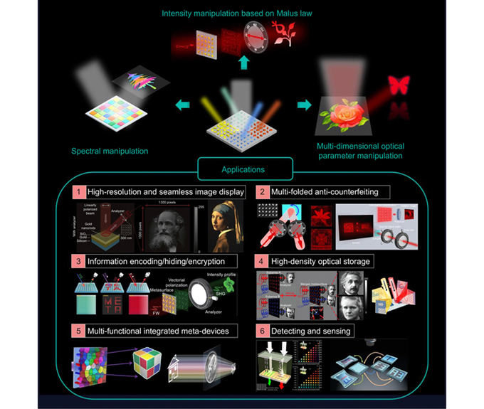
    Fig. 1. Overview of metasurface-based nanoprinting and its typical applications.
    Metasurface-based intensity manipulation based on Malus law. (a) Diagram of the unit-cell of a metasurface. (b) Illustration of arbitrary amplitude/intensity manipulation based on metasurface.
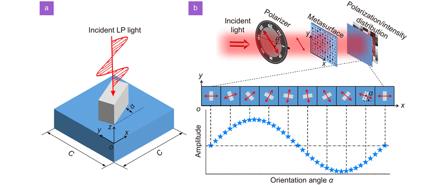
    Fig. 2. Metasurface-based intensity manipulation based on Malus law. (a) Diagram of the unit-cell of a metasurface. (b) Illustration of arbitrary amplitude/intensity manipulation based on metasurface.
    Three main physical resonances for generating structural-colors. (a) A metallic sphere supporting LSPR. (b) A high-refractive-index dielectric sphere supporting Mie resonance. (c) Schematic of constructive interference in F-P cavity.
    Fig. 3. Three main physical resonances for generating structural-colors. (a) A metallic sphere supporting LSPR. (b) A high-refractive-index dielectric sphere supporting Mie resonance. (c) Schematic of constructive interference in F-P cavity.
    Advanced applications empowered by single-channel meta-nanoprinting. (a, b) Continuous grayscale image display with high resolution. (c) Information encryption/concealing. Figure reproduced with permission from: (a) ref.19, under the terms of the Creative Commons CC BY license; (b) ref. 20, under the terms of the OSA Open Access Publishing Agreement; (c) ref.21, John Wiley and Sons.
    Fig. 4. Advanced applications empowered by single-channel meta-nanoprinting. (a, b) Continuous grayscale image display with high resolution. (c) Information encryption/concealing. Figure reproduced with permission from: (a) ref.19, under the terms of the Creative Commons CC BY license; (b) ref. 20, under the terms of the OSA Open Access Publishing Agreement; (c) ref.21, John Wiley and Sons.
    Metasurface-based nanoprinting explored in nonlinear optical regime for optical encoding/encryption. (a) A nonlinear photonic metasurface composed of meta-atoms with threefold rotational symmetry. (b) A Malus metasurface composed of gold nanostructures with threefold rotational symmetry. (c) A methyl ammonium lead tri-bromide perovskite metasurface with enhancing three-photon luminescence through nonlinear resonance. Figure reproduced with permission from: (a) ref.26, American Chemical Society; (b) ref.27, American Physical Society; (c) ref. 28, under the terms of the Creative Commons CC BY license.
    Fig. 5. Metasurface-based nanoprinting explored in nonlinear optical regime for optical encoding/encryption. (a) A nonlinear photonic metasurface composed of meta-atoms with threefold rotational symmetry. (b) A Malus metasurface composed of gold nanostructures with threefold rotational symmetry. (c) A methyl ammonium lead tri-bromide perovskite metasurface with enhancing three-photon luminescence through nonlinear resonance. Figure reproduced with permission from: (a) ref.26, American Chemical Society; (b) ref.27, American Physical Society; (c) ref. 28, under the terms of the Creative Commons CC BY license.
    Orthogonal-polarization multiplexed multi-channel grayscale nanoprinting. (a) Coherent pixel strategy used to realize multiple nanoprinting-image switching based on multidimensional control of arbitrary optical parameters. (b) A chiral Malus metasurface composed of two stepped V-shaped chiral nanoaperture enantiomers used for chiral grayscale nanoprinting-image display. (c) An alignment-free bilayer metasurface designed for polarization-encoded imaging. (d) Hyperbolic metamaterials (HMMs) employed to realize 2-bit intensity coding. Figure reproduced with permission from: (a) ref.65, John Wiley and Sons; (b) ref.66, John Wiley and Sons; (c) ref.67, John Wiley and Sons; (d) ref.68, American Chemical Society.
    Fig. 6. Orthogonal-polarization multiplexed multi-channel grayscale nanoprinting. (a) Coherent pixel strategy used to realize multiple nanoprinting-image switching based on multidimensional control of arbitrary optical parameters. (b) A chiral Malus metasurface composed of two stepped V-shaped chiral nanoaperture enantiomers used for chiral grayscale nanoprinting-image display. (c) An alignment-free bilayer metasurface designed for polarization-encoded imaging. (d) Hyperbolic metamaterials (HMMs) employed to realize 2-bit intensity coding. Figure reproduced with permission from: (a) ref.65, John Wiley and Sons; (b) ref.66, John Wiley and Sons; (c) ref.67, John Wiley and Sons; (d) ref.68, American Chemical Society.
    Non-orthogonal polarization-multiplexed multi-channel grayscale nanoprinting. (a) A 3D Janus metasurface used for non-orthogonal polarization-encrypted data storage. (b) A dual-channel anti-counterfeiting metasurface based on orientation degeneracy of nanostructures. (c) Vectorial compound metapixels for image multiplexing and hiding with arbitrary non-orthogonal polarization. (d) A dual-channel Malus metasurface with single-pixel imaging (SPI) encryption. Figure reproduced from: (a) ref.69, under the terms of the Creative Commons CC BY license; (b) ref.70, American Chemical Society; (c) ref.75, John Wiley and Sons; (d) ref.76, American Association for the Advancement of Science.
    Fig. 7. Non-orthogonal polarization-multiplexed multi-channel grayscale nanoprinting. (a) A 3D Janus metasurface used for non-orthogonal polarization-encrypted data storage. (b) A dual-channel anti-counterfeiting metasurface based on orientation degeneracy of nanostructures. (c) Vectorial compound metapixels for image multiplexing and hiding with arbitrary non-orthogonal polarization. (d) A dual-channel Malus metasurface with single-pixel imaging (SPI) encryption. Figure reproduced from: (a) ref.69, under the terms of the Creative Commons CC BY license; (b) ref.70, American Chemical Society; (c) ref.75, John Wiley and Sons; (d) ref.76, American Association for the Advancement of Science.
    One-dimensional subwavelength metallic gratings for color filtering. (a) Schematic diagram of the subwavelength Al-ZnSe-Al nano-resonator. Scale bar, 1 μm. (b) Measured transmission spectral response (blue, green and red) of the nanostructure shown in (a). (c) Schematic of the metallic grating structure with a buffer layer and a waveguide layer. (d) Simulated transmission spectra (blue, green and red) generated from the structure shown in (c). (e) Schematic of the high-performance color filters based on plasmonic metamirror. (f) Measured reflective spectra of the structure shown in (e). (g) Schematic diagram of the silver-grating color filters with varied periodicities. (h) Measured transmission spectral response (yellow, magenta and cyan) of the structure shown in (g). (i) Schematic of the metasurface- embedded nanocavity. (j) Comparison between the F-P resonator (utilizing two parallel mirrors) and the resonator with a reflective metasurface placed in two mirrors. Figure reproduced with permission from: (a, b) ref.91, Springer Nature; (c, d) ref.96, American Institute of Physics; (e, f) ref.98, De Gruyter; (g, h) ref.100, Springer Nature; (i, j) ref.106, under the terms of the Creative Commons CC BY license.
    Fig. 8. One-dimensional subwavelength metallic gratings for color filtering. (a) Schematic diagram of the subwavelength Al-ZnSe-Al nano-resonator. Scale bar, 1 μm. (b) Measured transmission spectral response (blue, green and red) of the nanostructure shown in (a). (c) Schematic of the metallic grating structure with a buffer layer and a waveguide layer. (d) Simulated transmission spectra (blue, green and red) generated from the structure shown in (c). (e) Schematic of the high-performance color filters based on plasmonic metamirror. (f) Measured reflective spectra of the structure shown in (e). (g) Schematic diagram of the silver-grating color filters with varied periodicities. (h) Measured transmission spectral response (yellow, magenta and cyan) of the structure shown in (g). (i) Schematic of the metasurface- embedded nanocavity. (j) Comparison between the F-P resonator (utilizing two parallel mirrors) and the resonator with a reflective metasurface placed in two mirrors. Figure reproduced with permission from: (a, b) ref.91, Springer Nature; (c, d) ref.96, American Institute of Physics; (e, f) ref.98, De Gruyter; (g, h) ref.100, Springer Nature; (i, j) ref.106, under the terms of the Creative Commons CC BY license.
    Two-dimensional plasmonic nanohole arrays for color filtering. (a) Schematic of the nanohole array structure arranged in square. (b) Optical microscopic images and scanning electron microscope (SEM) images of (a) with varied periodicities. (c) Schematic of the nanohole array structure arranged in triangle and the corresponding optical microscopic images and SEM images with varied periodicities. (d) Optical microscopic images and SEM images of the nanohole arrays with different shapes and lattices. (e) Schematic of the cross-shaped nanoaperture and the microscopic images of a butterfly with switchable colors under different LP light. Figure reproduced with permission from: (a, b) ref.124, Elsevier BV; (c) ref.125, under the terms of the Creative Commons CC BY license; (d) ref.127, American Institute of Physics; (e) ref.128, American Chemical Society.
    Fig. 9. Two-dimensional plasmonic nanohole arrays for color filtering. (a) Schematic of the nanohole array structure arranged in square. (b) Optical microscopic images and scanning electron microscope (SEM) images of (a) with varied periodicities. (c) Schematic of the nanohole array structure arranged in triangle and the corresponding optical microscopic images and SEM images with varied periodicities. (d) Optical microscopic images and SEM images of the nanohole arrays with different shapes and lattices. (e) Schematic of the cross-shaped nanoaperture and the microscopic images of a butterfly with switchable colors under different LP light. Figure reproduced with permission from: (a, b) ref.124, Elsevier BV; (c) ref.125, under the terms of the Creative Commons CC BY license; (d) ref.127, American Institute of Physics; (e) ref.128, American Chemical Society.
    Two-dimensional plasmonic nanorod arrays for color filtering. (a) Schematic of the cross-shaped nanorod. (b) Simulated transmission spectral response of the nanorods shown in (a), illuminated by LP light with polarization angles ranging from 0° to 90°. (c) Schematic illustration of the plasmonic pixels consisting of nanorods with different sizes and spacings. (d) Color palettes of merely size variations, and the mixing of size variations and spacing variations. (e) The realistic reproduction of artwork employing the expanded palette of colors. Scale bar, 50 μm. (f) Measured scattering spectra of the Fano-resonance-based nanocluster with varied diameters ranging from 110 nm to 40 nm. (g) Color detection of refractive index utilizing the localized surface plasmon resonance shift. Figure reproduced permission from: (a, b) ref.130, (c–e) ref.135, (f, g) ref.136, American Chemical Society.
    Fig. 10. Two-dimensional plasmonic nanorod arrays for color filtering. (a) Schematic of the cross-shaped nanorod. (b) Simulated transmission spectral response of the nanorods shown in (a), illuminated by LP light with polarization angles ranging from 0° to 90°. (c) Schematic illustration of the plasmonic pixels consisting of nanorods with different sizes and spacings. (d) Color palettes of merely size variations, and the mixing of size variations and spacing variations. (e) The realistic reproduction of artwork employing the expanded palette of colors. Scale bar, 50 μm. (f) Measured scattering spectra of the Fano-resonance-based nanocluster with varied diameters ranging from 110 nm to 40 nm. (g) Color detection of refractive index utilizing the localized surface plasmon resonance shift. Figure reproduced permission from: (a, b) ref.130, (c–e) ref.135, (f, g) ref.136, American Chemical Society.
    Two-dimensional silicon nanorod arrays for color filtering. (a) Schematic of all-dielectric color filters based on silicon nanodisks. (b) Schematic of the silicon nanobrick arrays, and the optical microscopic image of the fabricated nanobricks with different widths irradiated with LP light. (c) Schematic illustration of meta-nanoprinting to brighten structural-color by introducing dimethyl sulfoxide (DMSO). (d) Two different spectral responses and nanoprinting-images when the surrounding materials of the metasurface are air and DMSO, respectively. Figure reproduced with permission from: (a) ref.146, (b) ref.151, American Chemical Society; (c, d) ref.160, under the terms of the Creative Commons CC BY license.
    Fig. 11. Two-dimensional silicon nanorod arrays for color filtering. (a) Schematic of all-dielectric color filters based on silicon nanodisks. (b) Schematic of the silicon nanobrick arrays, and the optical microscopic image of the fabricated nanobricks with different widths irradiated with LP light. (c) Schematic illustration of meta-nanoprinting to brighten structural-color by introducing dimethyl sulfoxide (DMSO). (d) Two different spectral responses and nanoprinting-images when the surrounding materials of the metasurface are air and DMSO, respectively. Figure reproduced with permission from: (a) ref.146, (b) ref.151, American Chemical Society; (c, d) ref.160, under the terms of the Creative Commons CC BY license.
    Two-dimensional nanorod arrays based on other high-refractive-index dielectric materials for color filtering. (a) Schematic illustration, SEM image, and optical microscopic images of nanostructures with different geometries. (b) Schematic setup of the resonant laser printing. Nanostructures (i to ix) are generated by increasing the laser powers. (c) Schematic of the full-color nanopainting setup and the experimental color printing. Scale bar, 50 μm. (d) Color filtering based on the Si3N4 metasurface. Figure reproduced with permission from: (a, b) ref.149, under a Creative Commons AttributionNonCommercial License 4.0; (c) ref.165, Optical Society of America; (d) ref.167, American Chemical Society.
    Fig. 12. Two-dimensional nanorod arrays based on other high-refractive-index dielectric materials for color filtering. (a) Schematic illustration, SEM image, and optical microscopic images of nanostructures with different geometries. (b) Schematic setup of the resonant laser printing. Nanostructures (i to ix) are generated by increasing the laser powers. (c) Schematic of the full-color nanopainting setup and the experimental color printing. Scale bar, 50 μm. (d) Color filtering based on the Si3N4 metasurface. Figure reproduced with permission from: (a, b) ref.149, under a Creative Commons AttributionNonCommercial License 4.0; (c) ref.165, Optical Society of America; (d) ref.167, American Chemical Society.
    Two-dimensional multi-layer hybrid nanostructure arrays for color filtering. (a) Configuration of the hybrid nanodisks for subtractive color filtering (cyan, magenta and yellow). (b) Measured reflection spectrum and optical microscopic images of hybrid nanodisks with varied diameters. (c) SEM images of the fabricated samples with different diameters. Scale bar, 250 nm. (d) Structural design of the multi-dielectric metasurface. (e) Measured reflection spectra and optical microscopic images of the multi-dielectric metasurface with varied periodicities and gaps. Figure reproduced with permission from: (a–c) ref.176, John Wiley and Sons; (d, e) ref.178, American Chemical Society.
    Fig. 13. Two-dimensional multi-layer hybrid nanostructure arrays for color filtering. (a) Configuration of the hybrid nanodisks for subtractive color filtering (cyan, magenta and yellow). (b) Measured reflection spectrum and optical microscopic images of hybrid nanodisks with varied diameters. (c) SEM images of the fabricated samples with different diameters. Scale bar, 250 nm. (d) Structural design of the multi-dielectric metasurface. (e) Measured reflection spectra and optical microscopic images of the multi-dielectric metasurface with varied periodicities and gaps. Figure reproduced with permission from: (a–c) ref.176, John Wiley and Sons; (d, e) ref.178, American Chemical Society.
    Dynamically tunable colors with external stimulus. (a) Schematic of the plasmonic-LC pixel with/without applied voltages. (b) Measured optical microscopic images of the plasmonic-LC pixels with varied periodicities and electric fields. (c) Experimentally captured images of a singular Afghan Girl image with different electric fields. Scale bar, 100 μm. (d) Schematic of the electrically tunable color filter. (e) Model of the composite nanostructure, and the measured optical microscopic images at 20 °C and 80 °C, respectively. (f) Schematic of the plasmonic metasurface composed of hydrogen-responsive magnesium (Mg) nanobricks. (g) Optical microscopic images of the Minerva logo during hydrogenation and dehydrogenation for color erasing and restoring. Scale bar, 20 μm. (h) Schematic of polydimethylsiloxane relief with multiple states of color images revealed by directional strains and capillary force. Figure reproduced with permission from: (a–c) ref.193, under the terms of the Creative Commons CC BY license; (d) ref.194, American Chemical Society; (e) ref.197, John Wiley and Sons; (f, g) ref.198, under the terms of the Creative Commons CC BY license; (h) ref.202, John Wiley and Sons.
    Fig. 14. Dynamically tunable colors with external stimulus. (a) Schematic of the plasmonic-LC pixel with/without applied voltages. (b) Measured optical microscopic images of the plasmonic-LC pixels with varied periodicities and electric fields. (c) Experimentally captured images of a singular Afghan Girl image with different electric fields. Scale bar, 100 μm. (d) Schematic of the electrically tunable color filter. (e) Model of the composite nanostructure, and the measured optical microscopic images at 20 °C and 80 °C, respectively. (f) Schematic of the plasmonic metasurface composed of hydrogen-responsive magnesium (Mg) nanobricks. (g) Optical microscopic images of the Minerva logo during hydrogenation and dehydrogenation for color erasing and restoring. Scale bar, 20 μm. (h) Schematic of polydimethylsiloxane relief with multiple states of color images revealed by directional strains and capillary force. Figure reproduced with permission from: (a–c) ref.193, under the terms of the Creative Commons CC BY license; (d) ref.194, American Chemical Society; (e) ref.197, John Wiley and Sons; (f, g) ref.198, under the terms of the Creative Commons CC BY license; (h) ref.202, John Wiley and Sons.
    Multifunctional metasurfaces integrating color nanoprinting and monochromatic holography. (a) A dual-mode metasurface by simultaneously controlling the spectral response and geometric phase. (b) A multifunctional metasurface (for color image and holographic image display) with the control of spectral response and propagation phase. (c) Left panel: schematic diagram of a unit-cell and the simulated reflective spectra of silicon nanobricks with varied dimensions. Right panel: multifunctional metasurface merging rich structural-color nanoprinting and holography. Figure reproduced with permission from: (a) ref.203, American Chemical Society; (b) ref.204, The Royal Society of Chemistry; (c) ref.205, Optical Society of America.
    Fig. 15. Multifunctional metasurfaces integrating color nanoprinting and monochromatic holography. (a) A dual-mode metasurface by simultaneously controlling the spectral response and geometric phase. (b) A multifunctional metasurface (for color image and holographic image display) with the control of spectral response and propagation phase. (c) Left panel: schematic diagram of a unit-cell and the simulated reflective spectra of silicon nanobricks with varied dimensions. Right panel: multifunctional metasurface merging rich structural-color nanoprinting and holography. Figure reproduced with permission from: (a) ref.203, American Chemical Society; (b) ref.204, The Royal Society of Chemistry; (c) ref.205, Optical Society of America.
    Multifunctional metasurfaces integrating color nanoprinting and color holography. (a) The detour phase used to encode color holographic images into color nanoprint. Inset (bottom right) shows three cone arrays with different cones’ dimensions to generate the desired reflection spectra. And the detour phase is employed to manipulate the phase. (b) Bicolor nanoprinting and holography within a single-layer dielectric metasurface by simultaneously modulating spectral and spatial responses. (c) Holographic color prints implemented by combining structural-color filters with phase plates. (d) Left panel: a supercell made of R, G and B double-nanoblock cells to control the amplitude and phase of incident R, G and B light separately. Right panel: Full-color nanoprint-hologram-integrated metasurface with arbitrary HSB control. (e) Simultaneous full-color nanoprinting and holography enabled by a plasmonic shallow grating (PSG) metasurface. (f) Left panel: dynamic bifunctional metasurface for switchable color nanoprinting and color holography. Right panel: schematic of Si nanopillar (top) and SEM image of the metasurface (bottom). Figure reproduced with permission from: (a) ref.207, John Wiley and Sons; (b) ref.208, American Chemical Society; (c) ref.209, (d) ref.210, (e) ref.211, (f) ref. 212, under the terms of the Creative Commons CC BY license.
    Fig. 16. Multifunctional metasurfaces integrating color nanoprinting and color holography. (a) The detour phase used to encode color holographic images into color nanoprint. Inset (bottom right) shows three cone arrays with different cones’ dimensions to generate the desired reflection spectra. And the detour phase is employed to manipulate the phase. (b) Bicolor nanoprinting and holography within a single-layer dielectric metasurface by simultaneously modulating spectral and spatial responses. (c) Holographic color prints implemented by combining structural-color filters with phase plates. (d) Left panel: a supercell made of R, G and B double-nanoblock cells to control the amplitude and phase of incident R, G and B light separately. Right panel: Full-color nanoprint-hologram-integrated metasurface with arbitrary HSB control. (e) Simultaneous full-color nanoprinting and holography enabled by a plasmonic shallow grating (PSG) metasurface. (f) Left panel: dynamic bifunctional metasurface for switchable color nanoprinting and color holography. Right panel: schematic of Si nanopillar (top) and SEM image of the metasurface (bottom). Figure reproduced with permission from: (a) ref.207, John Wiley and Sons; (b) ref.208, American Chemical Society; (c) ref.209, (d) ref.210, (e) ref.211, (f) ref. 212, under the terms of the Creative Commons CC BY license.
    Multifunctional metasurfaces integrating multi-nanoprinting and multi-holography. (a) Multifunctional metasurfaces enabled by independent controlling optical phase and amplitude in two orthogonally-polarized states. Inset: one super-pixel of the metasurface. (b) Top panel: triple sets of printing-hologram integrated into a single-layer metasurface with six DOFs. Bottom panel: the unit cell consists of four identical c-silicon nanoblocks with different x coordinate positions and orientation angles. (c) Top panel: a bifunctional metasurface combining structural-color nanoprinting and vectorial holography with eight polarization channels. Bottom panel: optical microscopic and SEM images of the fabricated metasurface. (d) Top panel: angular-multiplexing metasurface by building up independent-encoded amplitude/phase dictionary for angular illumination. Bottom panel: side view of the angle-multiplexing metasurface (left) and schematic diagram of an array structure (right). (e) Top panel: electric-driven dynamical near-/far-field multiplexing display. Bottom panel: schematic of the rectangular nanopillars with varied dimensions and SEM images of the sample. Figure reproduced from: (a) ref.213, under the terms of the Creative Commons CC BY license; (b) ref.214, under a Creative Commons Attribution NonCommercial License 4.0; (c) ref.215, under the terms of the Creative Commons CC BY license; (d) ref.216, (e) ref.217, John Wiley and Sons.
    Fig. 17. Multifunctional metasurfaces integrating multi-nanoprinting and multi-holography. (a) Multifunctional metasurfaces enabled by independent controlling optical phase and amplitude in two orthogonally-polarized states. Inset: one super-pixel of the metasurface. (b) Top panel: triple sets of printing-hologram integrated into a single-layer metasurface with six DOFs. Bottom panel: the unit cell consists of four identical c-silicon nanoblocks with different x coordinate positions and orientation angles. (c) Top panel: a bifunctional metasurface combining structural-color nanoprinting and vectorial holography with eight polarization channels. Bottom panel: optical microscopic and SEM images of the fabricated metasurface. (d) Top panel: angular-multiplexing metasurface by building up independent-encoded amplitude/phase dictionary for angular illumination. Bottom panel: side view of the angle-multiplexing metasurface (left) and schematic diagram of an array structure (right). (e) Top panel: electric-driven dynamical near-/far-field multiplexing display. Bottom panel: schematic of the rectangular nanopillars with varied dimensions and SEM images of the sample. Figure reproduced from: (a) ref.213, under the terms of the Creative Commons CC BY license; (b) ref.214, under a Creative Commons Attribution NonCommercial License 4.0; (c) ref.215, under the terms of the Creative Commons CC BY license; (d) ref.216, (e) ref.217, John Wiley and Sons.
    Multifunctional metasurfaces integrating nanoprinting and holography based on nanocavity. (a) Integrated metasurface with tricolor nanoprinting and helicity-multiplexed holograms for real-time optical encryption. (b) Mg-based metasurface for dual-function switching between color display and holography. (c) Stepwise nanocavities for nanoprint-hologram displays. (d) Stepwise dual-Fabry-Pérot (DF-P) nanocavity for grayscale imaging encryption/concealment with holographic multiplexing. Figure reproduced with permission from: (a) ref.219, John Wiley and Sons; (b) ref.220, American Chemical Society; (c) ref.221, (d) ref.222, John Wiley and Sons.
    Fig. 18. Multifunctional metasurfaces integrating nanoprinting and holography based on nanocavity. (a) Integrated metasurface with tricolor nanoprinting and helicity-multiplexed holograms for real-time optical encryption. (b) Mg-based metasurface for dual-function switching between color display and holography. (c) Stepwise nanocavities for nanoprint-hologram displays. (d) Stepwise dual-Fabry-Pérot (DF-P) nanocavity for grayscale imaging encryption/concealment with holographic multiplexing. Figure reproduced with permission from: (a) ref.219, John Wiley and Sons; (b) ref.220, American Chemical Society; (c) ref.221, (d) ref.222, John Wiley and Sons.
    Multifunctional metasurfaces integrating nanoprinting and holography based on orientation degeneracy of anisotropic nanostructures. (a) Schematic of the bifunctional metasurface consisting of single-sized nanostructures. (b) Tri-channel metasurface for simultaneous meta-holography and meta-nanoprinting with a single-cell design approach. (c) Tri-functional metasurface enabled by triple manipulations of light. (d) Tri-channel metasurface for dual-channel polychromatic nanoprinting-image displays and single-channel polychromatic holographic image display. (e) Multifold integration of nanoprinting and holography enabled by dual-degeneracy of nanostructures. Figure reproduced from: (a) ref. 224, The Author(s); (b) ref. 225, WILEY-VCH Verlag GmbH & Co. KGaA, Weinheim; (c) ref. 226, WILEY-VCH Verlag GmbH & Co. KGaA, Weinheim; (d) ref. 227, Renyuan Ren et al., published by De Gruyter under the Creative Commons Attribution 4.0 Public License; (e) ref. 229, Wiley-VCH GmbH.
    Fig. 19. Multifunctional metasurfaces integrating nanoprinting and holography based on orientation degeneracy of anisotropic nanostructures. (a) Schematic of the bifunctional metasurface consisting of single-sized nanostructures. (b) Tri-channel metasurface for simultaneous meta-holography and meta-nanoprinting with a single-cell design approach. (c) Tri-functional metasurface enabled by triple manipulations of light. (d) Tri-channel metasurface for dual-channel polychromatic nanoprinting-image displays and single-channel polychromatic holographic image display. (e) Multifold integration of nanoprinting and holography enabled by dual-degeneracy of nanostructures. Figure reproduced from: (a) ref. 224, The Author(s); (b) ref. 225, WILEY-VCH Verlag GmbH & Co. KGaA, Weinheim; (c) ref. 226, WILEY-VCH Verlag GmbH & Co. KGaA, Weinheim; (d) ref. 227, Renyuan Ren et al., published by De Gruyter under the Creative Commons Attribution 4.0 Public License; (e) ref. 229, Wiley-VCH GmbH.
    Multifunctional metasurfaces integrating nanoprinting and metalens. (a) Left panel: diagrams of a transmission unit (top) and a reflection unit (bottom). Right panel: coplanar metalens embedded into nanoprinted display. (b) Left panel: schematic illustration of a unit-cell (top) and the principle of intensity and phase manipulation. Right panel: metasurface decoupling for near- and far-field functionalizations of nanoprinting and metalens. Figure reproduced with permission from: (a) ref.230, American Chemical Society; (b) ref.231, John Wiley and Sons.
    Fig. 20. Multifunctional metasurfaces integrating nanoprinting and metalens. (a) Left panel: diagrams of a transmission unit (top) and a reflection unit (bottom). Right panel: coplanar metalens embedded into nanoprinted display. (b) Left panel: schematic illustration of a unit-cell (top) and the principle of intensity and phase manipulation. Right panel: metasurface decoupling for near- and far-field functionalizations of nanoprinting and metalens. Figure reproduced with permission from: (a) ref.230, American Chemical Society; (b) ref.231, John Wiley and Sons.
    Working typeUnit cellPeak efficiencyModulation mechanismPixel sizeColor gamut (sRGB)Ref.
    TransmissionAluminium slitR(~51%)Varying geometryR(360 nm)Unreportedref.91
    G(~62%)G(270 nm)
    B(~45%)B(230 nm)
    ReflectionSilver slitR(~73%)Varying geometryR(590 nm)Unreportedref.98
    G(~75%)G(470 nm)
    B(~63%)B(300 nm)
    TransmissionSilver slit60~70%Varying geometryC(350 nm)Unreportedref.100
    M(270 nm)
    Y(230 nm)
    TransmissionAluminium triangular nanohole~37%Varying geometryR(420 nm)Unreportedref.127
    G(340 nm)
    B(300 nm)
    TransmissionAluminum cross-shaped nanoaperture 5~12%Varying geometry250~340 nmUnreportedref.128
    ReflectionSilver tandem nanodisk~60%Varying geometry200~400 nmUnreportedref.133
    ReflectionAluminium circular nanodisk>75%Varying geometry320 nm~45%ref.134
    ReflectionAluminium circular nanorod~80%Varying geometry800 nm>300 colorsref.135
    ReflectionSilicon circular nanodiskR(~66%)Varying geometry250 nm~78%ref.150
    G(~49%)
    B(~31%)
    ReflectionSilicon nanobrick50~75%Varying geometry300 nmUnreportedref.151
    ReflectionSilicon circular nanodisk30~82%Varying geometry110~320 nm181%ref.160
    TransmissionTitanium dioxide elliptical nanopillars R(~83%)Varying geometry1110×740 nmUnreportedref.165
    G(~86%)
    B(~81%)
    ReflectionSilicon nitride nanobrickR(~91%)Varying geometry295~435 nmComparable to sRGBref.167
    G(~92%)
    B(~91%)
    ReflectionMulti-dielectric nanobrick~93%Varying geometry300~400 nm171%ref.178
    ReflectionPlasmonic-liquid crystal cell~75%Applied voltages300 nmUnreportedref.193
    ReflectionSilver circular nanodisk20~25%Temperature300 nmUnreportedref.197
    ReflectionHydrogen-responsive magnesium nanobrick 20~40%Hydrogenation & dehydrogenation 170~500 nmUnreportedref.198
    TransmissionPolydimethylsiloxane slit~60%Directional strains & capillary forces 1500 nmUnreportedref.202
    Table 1. Performance comparison of typical references for color nanoprinting.
    Rao Fu, Kuixian Chen, Zile Li, Shaohua Yu, Guoxing Zheng. Metasurface-based nanoprinting: principle, design and advances[J]. Opto-Electronic Science, 2022, 1(10): 220011
    Download Citation