Journals >Opto-Electronic Science
Contents


2022
Volume: 1 Issue 10
2 Article(s)
Export citation format
Research Articles

Metasurface-based nanoprinting: principle, design and advances
Rao Fu, Kuixian Chen, Zile Li, Shaohua Yu, and Guoxing Zheng
Metasurface-based nanoprinting (meta-nanoprinting) has fully demonstrated its advantages in ultrahigh-density grayscale/color image recording and display. A typical meta-nanoprinting device usually has image resolutions reaching 80 k dots per inch (dpi), far exceeding conventional technology such as gravure printing (t![]()
Metasurface-based nanoprinting (meta-nanoprinting) has fully demonstrated its advantages in ultrahigh-density grayscale/color image recording and display. A typical meta-nanoprinting device usually has image resolutions reaching 80 k dots per inch (dpi), far exceeding conventional technology such as gravure printing (typ. 5 k dpi). Besides, by fully exploiting the design degrees of freedom of nanostructured metasurfaces, meta-nanoprinting has been developed from previous single-channel to multiple-channels, to current multifunctional integration or even dynamic display. In this review, we overview the development of meta-nanoprinting, including the physics of nanoprinting to manipulate optical amplitude and spectrum, single-functional meta-nanoprinting, multichannel meta-nanoprinting, dynamic meta-nanoprinting and multifunctional metasurface integrating nanoprinting with holography or metalens, etc. Applications of meta-nanoprinting such as image display, vortex beam generation, information decoding and hiding, information encryption, high-density optical storage and optical anti-counterfeiting have also been discussed. Finally, we conclude the opportunities and challenges/perspectives in this rapidly developing research field of meta-nanoprinting..
Opto-Electronic Science
- Publication Date: Oct. 28, 2022
- Vol. 1, Issue 10, 220011 (2022)


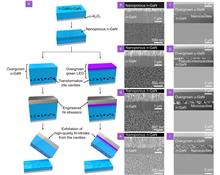
Large-scale and high-quality III-nitride membranes through microcavity-assisted crack propagation by engineering tensile-stressed Ni layers
Jung-Hong Min, Kwangjae Lee, Tae-Hoon Chung, Jung-Wook Min... and Boon S. Ooi|Show fewer author(s)
Epitaxially grown III-nitride alloys are tightly bonded materials with mixed covalent-ionic bonds. This tight bonding presents tremendous challenges in developing III-nitride membranes, even though semiconductor membranes can provide numerous advantages by removing thick, inflexible, and costly substrates. Herein, cavi![]()
Epitaxially grown III-nitride alloys are tightly bonded materials with mixed covalent-ionic bonds. This tight bonding presents tremendous challenges in developing III-nitride membranes, even though semiconductor membranes can provide numerous advantages by removing thick, inflexible, and costly substrates. Herein, cavities with various sizes were introduced by overgrowing target layers, such as undoped GaN and green LEDs, on nanoporous templates prepared by electrochemical etching of n-type GaN. The large primary interfacial toughness was effectively reduced according to the design of the cavity density, and the overgrown target layers were then conveniently exfoliated by engineering tensile-stressed Ni layers. The resulting III-nitride membranes maintained high crystal quality even after exfoliation due to the use of GaN-based nanoporous templates with the same lattice constant. The microcavity-assisted crack propagation process developed for the current III-nitride membranes forms a universal process for developing various kinds of large-scale and high-quality semiconductor membranes..
Opto-Electronic Science
- Publication Date: Oct. 28, 2022
- Vol. 1, Issue 10, 220016 (2022)


© Copyright 2018-2021 | Chinese Laser Press. All Rights Reserved 沪ICP备15018463号-20