Abstract
![]()
Metasurface-based nanoprinting (meta-nanoprinting) has fully demonstrated its advantages in ultrahigh-density grayscale/color image recording and display. A typical meta-nanoprinting device usually has image resolutions reaching 80 k dots per inch (dpi), far exceeding conventional technology such as gravure printing (typ. 5 k dpi). Besides, by fully exploiting the design degrees of freedom of nanostructured metasurfaces, meta-nanoprinting has been developed from previous single-channel to multiple-channels, to current multifunctional integration or even dynamic display. In this review, we overview the development of meta-nanoprinting, including the physics of nanoprinting to manipulate optical amplitude and spectrum, single-functional meta-nanoprinting, multichannel meta-nanoprinting, dynamic meta-nanoprinting and multifunctional metasurface integrating nanoprinting with holography or metalens, etc. Applications of meta-nanoprinting such as image display, vortex beam generation, information decoding and hiding, information encryption, high-density optical storage and optical anti-counterfeiting have also been discussed. Finally, we conclude the opportunities and challenges/perspectives in this rapidly developing research field of meta-nanoprinting.
Introduction
Conventional optical devices made of natural materials exhibit bulky volumes, which cannot accord with the current trend of device miniaturization and hence hinders the development of ultra-compact optical systems. Ever since the excellent phase control of a metasurface was first demonstrated by Capasso’s group in 20111, metasurface serves as a promising candidate for substituting conventional optical components to realize an ultra-compact nano-photonics system, taking account of its extraordinary light manipulation ability and dramatically reduced device thickness. Due to the high efficiency of phase-only devices, from the beginning, vast research endeavors have been focused on demonstrating meta-devices that can realize various wavefront shaping functionalities, such as metalens2-8, meta-hologram9-13, vortex beam generator14-18 and so on.
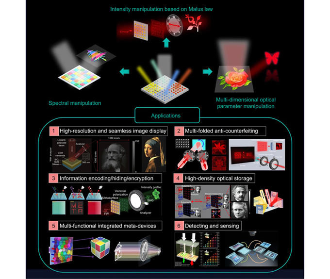
Apart from the phase feature, amplitude is another fundamental optical property that plays an invaluable role in affecting the strength of light-matter interaction. Over the past decade, metasurface-based nanoprinting (meta-nanoprinting)19-28, a novel technology to realize the grayscale/color nanoprinting-image record/display with high resolution, has been extensively explored all over the world. Thanks to the subwavelength nanostructure/meta-atom and the ability of precise amplitude/spectrum modulation, meta-nanoprinting has the advantages of high image resolution, delicate color exhibition, high-stability and high information density. Therefore, it is of great significance and potential in applications including high-resolution image display19-20, information encryption/concealing21-24 and multi-folded anti-counterfeiting25 , to name a few, as shown in Fig. 1.

Figure 1.Overview of metasurface-based nanoprinting and its typical applications.
Although there have been several review articles closely related to metasurface-based nanoprinting29-40, which mainly focused on artificial structural colors generation, we believe a comprehensive review about the technology of meta-nanoprinting will be beneficial to the community. In this review, we start from the principles of realizing meta-nanoprinting, including polarization-dependent intensity manipulation based on Malus law and spectrum-dependent structural-color generation. Then, we introduce various design strategies to achieve single-functional meta-nanoprinting and the generation of meta-devices that can fulfill multiple functionalities (nanoprinting and holography/lens) on a single metasurface platform, as well as their applications. Finally, we discuss and conclude the future development/opportunities and challenges/perspectives in this rapidly developing research field of meta-nanoprinting.
Physics behind meta-nanoprinting
In traditional optics, amplitude is modulated by controlling local transmission or reflection coefficient of optical medium. Similarly, for metasurface, amplitude manipulation can also be achieved by locally adjusting the reflection or transmission properties41-44. The simplest one is binary amplitude modulation, that is, amplitude modulation of two reflected values or two transmitted values. However, the effect of binary amplitude modulation is limited. To carry more information, it is necessary to increase the number of steps for amplitude control. Therefore, a variety of principles have been proposed to realize more precise amplitude/intensity modulation. For example, inspired by detour phase encoding, detour phase metasurfaces45-47 have been proposed to realize multi-step amplitude modulation by changing the width45, 46 or number47 of slits in each pixel and continuous phase modulation by adjusting the positions of the slits. Subsequently, nanostructures with cross sections of V-shape48, C-shape49, I-shape50 and rectangle-shape51 have been theoretically demonstrated to achieve continuous amplitude manipulation by varying the sizes of nanostructures. However, considering the fabrication accuracy, these approaches can only achieve stepped amplitude manipulation in fact.
For meta-nanoprinting, a printing technology to record/display image, it is eager to obtain continuous intensity control or full color control, thus the physics behind meta-nanoprinting can be classified into two main categories: polarization-assisted intensity manipulation based on Malus law, and spectrum manipulation based on structural-colors. Beside the difference in working principle, the strategies to generate color are also different. The first one generally requires three different nanostructures with narrowband responses to generate three primary colors (red, green and blue) respectively, and then performs color mixing, working like the commercial liquid-crystal-based screen. For the second one, each nanostructure has its unique response spectra, therefore corresponding to a unique color. We describe their working principles below.
Polarization-assisted intensity manipulation based on Malus law
Due to the characteristic of continuous amplitude control, polarization-assisted intensity manipulation based on Malus law has aroused a wide concern. According to the classic Malus law, when linearly polarized (LP) light with intensity of I0 passes through a linearly bulk-optic polarizer, the transmitted light intensity (ignoring the absorption) can be expressed as I=I0cos²θ, where θ is the angle between the polarization direction of the incident LP light and the transmission axis of the polarizer. Malus law can be introduced into metasurface community to control the polarization-assisted intensity pixel-by-pixel, thus building the intensity-modulated nanoprinting.
Specifically, taking an anisotropic nanostructure with rectangular cross section for example, as shown in Fig. 2(a), its Jones matrix can be described as
Figure 2.Metasurface-based intensity manipulation based on Malus law. (a) Diagram of the unit-cell of a metasurface. (b) Illustration of arbitrary amplitude/intensity manipulation based on metasurface.
where A and D represent the complex transmission/reflection coefficients for incident light waves polarized along two orthogonal directions (i.e., the short and long axes), respectively. By elaborately adjusting geometry parameters of the nanostructure, it can be designed as an arbitrary polarization element with subwavelength feature, such as a linear polarizer, a half-wave plate (HWP), a quarter-wave plate and so on, which can change the polarization state of the incident light. On this basis, applying the rotation parameters to the nanostructure, the Jones matrix can be described as
where α is the orientation angle with respect to the x-axis of a nanostructure. For example, when LP light is incident on a nanostructure acting as a linear polarizer (i.e., A=1, D=0), the Jones vector of the output LP light can be written as
where θ1 represents the polarization angle (the angle between the polarization direction and the x-axis, as shown in Fig. 2(b)) of the incident LP light. Equation (3) indicates that the polarization angle of the output light equals the orientation angle of the nanostructure. More importantly, a continuous amplitude modulation can be achieved by varying the orientation angle α. This is the basic principle of polarization-assisted intensity modulation based on Malus law.
Consider another common case: adding an analyzer behind the nanostructure, the Jones vector of the output light can be written as
where θ2 denotes the angle between the transmission axis of the analyzer and the x-axis. In particular, the nanostructure is placed in an orthogonal-polarization optical path (i.e., θ1= 0°, θ2= 90°), we can readily simply the Eq. (4) to
It can be seen from Eq. (5) that the amplitude of the output LP light with Jones vector of
can be continuously modulated by rotating the orientation angle of the nanostructure.
The above-mentioned metasurface based on Malus law to achieve amplitude/intensity control, so-called Malus metasurface, is often composed of nanostructures with identical geometric size but varied orientation. It provides a simple and ingenious method for manipulating amplitude at the subwavelength scale. Additionally, the design complexity and fabrication difficulty are significantly reduced. More importantly, as shown in Eq. (5), the amplitude control is only related to the orientation of the nanostructure, and is irrelevant to the specific sizes of the nanostructure (as long as it is anisotropic) and the wavelength, so it has the characteristics of strong robustness against fabrication errors and broadband operation.
Spectrum manipulation to generate structural-colors
Various optical resonances arising from subwavelength nanostructures are attractive for the generation of structural-colors, which can be simply tailored by tuning their geometric dimensions. Here, as indicated in Fig. 3, three main categories of optical resonances are illustrated, including localized surface plasmon resonance (LSPR)29, Mie resonance52, 53 and Fabry-Pérot (F-P) resonance54-56.
Figure 3.Three main physical resonances for generating structural-colors. (a) A metallic sphere supporting LSPR. (b) A high-refractive-index dielectric sphere supporting Mie resonance. (c) Schematic of constructive interference in F-P cavity.
LSPR in metallic nanostructures shown in Fig. 3(a) is a natural approach to generate structural-colors29. Quasiparticles, called plasmons, are formed by the strong couple between the collective oscillation of free electrons and external electromagnetic waves, causing absorption and scattering of light at the resonance frequency which covers several hundreds of nanometers in the wavelength range. The resulting structural-colors originate from these resonance frequencies, which can be manipulated by varying the shape, geometries and the surrounding environment of nanostructures. Although metal material is widely employed in plasmonic color printing, its inherent ohmic losses would affect the optical resonances, thus leading to a limit of the generated color gamut. An alternative approach is to utilize the Mie resonance, which exists in dielectric materials with relatively low optical losses, as depicted in Fig. 3(b). Nanostructures made of high-refractive-index dielectrics (such as silicon) can work as Mie resonators. The fundamental multipoles of electric dipole and magnetic dipole can trigger Mie resonance with high quality factor52, 53. Owing to the lower intrinsic loss of dielectrics and sharp resonance, the structural-colors based on Mie resonance have a high color saturation and cover a broader color gamut compared to the plasmonic counterparts. Apart from aforementioned optical resonances, vivid and saturated structural-colors can also be obtained via an F-P cavity54, 55, as shown in Fig. 3(c). Constructive and destructive interferences occur as a result of light multi-reflection between the top and bottom interfaces of the F-P cavity. By varying the thickness of the F-P cavity to fit integer multiples of half wavelengths of constructive interference, the spectral response can be manipulated.
Single-functional meta-nanoprinting
Grayscale nanoprinting
Single-channel grayscale nanoprinting
In 2018, Yue et al. designed a metal-insulator-metal (MIM) nanostructure acting as an HWP and encoded a 256-level grayscale image as polarization state distribution with spatial variation19, which can be recorded by a Malus metasurface, as shown in Fig. 4(a). When LP light is incident on the metasurface, an inhomogeneous polarization distribution is generated, however, the intensity of the reflected light is evenly distributed. As a result, a grayscale image can be hidden in the vector laser beam with spatially variant polarization states. Only by adding an external linear polarizer in the reflected light path, can the hidden nanoprinting-image be revealed with high-resolution. Beside HWP, other polarization elements such as nano-polarizer can also be employed to record grayscale images. In 2019, Dai et al. designed a dielectric nano-polarizer structure by elaborately employing the magnetic resonance effect occurring in the dielectric nanobricks20. The incident light with polarization direction parallel to the short axis of the nanobrick can be transmitted, while its orthogonal counterpart will be strongly reflected. In this consideration, each nanostructure acts as a polarization sensitive pixel to construct a displayer at the subwavelength scale. According to Malus law, a continuous grayscale image can be encoded as the orientation distribution of nanobrick arrays. Therefore, the grayscale image display with resolutions up to 84667 dots per inch (dpi) is achieved, as shown in Fig. 4(b). Moreover, the nanoprinting-image is invisible under the natural light illumination with random polarization direction due to the homogeneous intensity distribution. A clear image with abundant grayscale information only appears when the incident beam is polarized along the x-axis.
Figure 4.Advanced applications empowered by single-channel meta-nanoprinting. (a, b) Continuous grayscale image display with high resolution. (c) Information encryption/concealing. Figure reproduced with permission from: (a) ref.19, under the terms of the Creative Commons CC BY license; (b) ref. 20, under the terms of the OSA Open Access Publishing Agreement; (c) ref.21, John Wiley and Sons.
Malus metasurface with polarization control shows great potential in optical information security/encryption and anti-counterfeiting. As shown in Fig. 4(c), in 2018, Zhao et al. proposed a polarization conversion metasurface, which can locally modify the polarization states of incident light, to generate arbitrary radial and azimuthal polarization beams with efficiencies up to 80%21. In addition, it can also implement polarization encryption of information, which is demonstrated by encoding an image pattern into the spatial inhomogeneous polarization distribution. The hidden image cannot be distinguished in laser beam without extra analysis of the Stokes parameters. In 2019, Xue et al. utilized the structural and thermal perturbations in the compound nanosieves, presenting a perturbation-induced countersurveillance strategy to realize information hiding with high security24. The message sender uses perturbation 1 to hide the important information in a color nanoprinting-image. After the receiver receives the information carrier, he needs to load perturbation 2 to it to make the hidden information and the background appear a small spectral shift, and then a specific optical filter is needed to read the hidden information. In addition to information hiding, as the loading process of perturbation 2 brings irreversible graph changes to the color nanoprinting-image as camouflage, this strategy can also be used for self-indicating whether the hidden information has been attacked during delivery. In this way, the information camouflage carrier acts as a self-monitoring indicator, that is, when the receiver receives the information carrier, if the camouflage graph changes, it indicates that the hidden information has been stolen.
Apart from polarization dependence, for Malus metasurfaces, there exists a unique feature that an intensity value corresponds to multiple orientation angles on account of Malus law, so called orientation degeneracy (OD). In 2020, Zhang et al. applied the concept of OD and presented nanoprinting-image display and encryption method by employing anisotropic silver (Ag) nano-polarizers considered as pixels22. For each pixel, there are two orientation angle options corresponding to an equal grayscale value. By randomly selecting the orientation angle between two choices, the nanoprinting-image can be hidden. This encryption method is experimentally demonstrated by encoding a Lena image with pixels of 1000 × 1000 into a Malus metasurface and decoding/encrypting the image in a polarization-controlled optical setup.
The above-mentioned approaches have been widely explored in the linear optical regime. Moreover, the concept of nanoprinting can also be extended to the field of nonlinear optics26-28. Nonlinear optical encryption involves nonlinear frequency conversions, representing a new strategy for securing optical information. In 2017, Walter et al. proposed a nonlinear photonic metasurface composed of meta-atoms with threefold rotational symmetry26, as shown in Fig. 5(a). One unit-cell (pixel) of the metasurface contains two meta-atoms with identical dimensions. The second harmonic generation (SHG) signal from the two neighboring meta-atoms will interfere and lead to a rotation angle dependent with the SHG intensity. When both meta-atoms have the same orientation angle, the SHG signal reaches a maximum due to the constructive interference. For other cases that the angles between them are different, it will result in a reduced SHG intensity. Therefore, the spatially variant control of the SHG signal can be realized by placing two neighboring meta-atoms with different orientation angles in the pixel. Such kind of nonlinear metasurface can be employed to hide optical images when incident light is a fundamental wave (FW). The hidden image can be read out under the illumination of SHG waves.
Figure 5.Metasurface-based nanoprinting explored in nonlinear optical regime for optical encoding/encryption. (a) A nonlinear photonic metasurface composed of meta-atoms with threefold rotational symmetry. (b) A Malus metasurface composed of gold nanostructures with threefold rotational symmetry. (c) A methyl ammonium lead tri-bromide perovskite metasurface with enhancing three-photon luminescence through nonlinear resonance. Figure reproduced with permission from: (a) ref.26, American Chemical Society; (b) ref.27, American Physical Society; (c) ref. 28, under the terms of the Creative Commons CC BY license.
In 2019, Tang et al. implemented nonlinear optical information encryption using Malus metasurface composed of gold nanostructures with threefold rotational symmetry27. By utilizing the nonlinear effect, the incident FW can be modulated into SHG, whose polarization state can be locally manipulated by changing the orientation angle of the nanostructure. Only by inserting an extra bulk-optic polarizer, can the vector polarization distribution of SHG be transformed into the intensity distribution, showing the encrypted optical image, as shown in Fig. 5(b). In the same year, Fan et al. fabricated methyl ammonium lead tri-bromide perovskite metasurfaces with specific resonant wavelength and realized high-resolution nonlinear nanoprinting and optical encryption by enhancing three-photon luminescence (TPL) through nonlinear resonance28. As shown in Fig. 5(c), the off-resonance pumping and the single-photon excitation just generate a uniform dark or photoluminescence background. The encoded information “NANO” can be revealed only when the incident laser is on-resonance. In this way, important information will be protected in transit and storage.
Multi-channel grayscale nanoprinting
Information multiplexing can make the maximal use of existing hardware facilities to improve the information capacity as much as possible without increased costs. For metasurfaces, with the aid of wavelength multiplexing57-59, angular multiplexing60, 61, spatial frequency multiplexing62, propagation direction multiplexing63 and polarization multiplexing64-78, multiple channels carrying different nanoprinting-image information can be recorded into one single metasurface, thus increasing the information capacity of meta-devices. Usually, information channels can be optically switched by altering the optical parameters, such as incident angle, wavelength, polarization and so on. Herein, we mainly focus on reviewing the advances in polarization multiplexed meta-nanoprinting, one of the most employed information multiplexing means for meta-nanoprinting.
By carefully optimizing the geometric dimensions of an anisotropic nanostructure, light waves with different polarization states can be manipulated independently. This design degree of freedom (DOF) can be employed to design polarization multiplexed metasurfaces. Multi-channel grayscale nanoprinting based on polarization multiplexed metasurface is usually implemented by a pair of orthogonally-polarized states64-68. For example, linearly polarization state along x/y axes or left/right-handed circularly polarization states can reveal different nanoprinting-images respectively.
In 2013, Wang et al. proposed the electrically pumped microscopic active display64, which consists of plasmonic nano-polarizer and light-emitting-diode (LED). Thanks to the strong modulation of the plasmonic rectangular nanoholes, polarization multiplexed binary letter encoding, single and double grayscale images and animation movies are successfully realized, which gives rise to flexible and controllable active display. This strategy indicates potential application in designing new type of microscopic electro-optical devices.
In 2018, Bao et al. employed the coherent pixel to realize multiple nanoprinting-image switching based on multidimensional control of arbitrary optical parameters (arbitrary incident angle, polarization, and wavelength)65. The coherent pixel is composed of several identical elements, as shown in Fig. 6(a), and all the elements as a whole contribute to the pixels of different images under different optical conditions. Considering that there are n elements in one pixel, when an incident beam with polarization σ, incident angle θ and wavelength λ is illuminated from the substrate side, the intensity of the pixel along z direction can be described as
Figure 6.Orthogonal-polarization multiplexed multi-channel grayscale nanoprinting. (a) Coherent pixel strategy used to realize multiple nanoprinting-image switching based on multidimensional control of arbitrary optical parameters. (b) A chiral Malus metasurface composed of two stepped V-shaped chiral nanoaperture enantiomers used for chiral grayscale nanoprinting-image display. (c) An alignment-free bilayer metasurface designed for polarization-encoded imaging. (d) Hyperbolic metamaterials (HMMs) employed to realize 2-bit intensity coding. Figure reproduced with permission from: (a) ref.65, John Wiley and Sons; (b) ref.66, John Wiley and Sons; (c) ref.67, John Wiley and Sons; (d) ref.68, American Chemical Society.
where xk is the x coordinate and φk denotes the orientation angle of the kth element. It can be seen from Eq. (6) that independent pixel intensity modulation can be realized by carefully adjusting the positions and orientation angles of elements within one pixel, which means multiple nanoprinting-images can be switched by varying different optical conditions. For example, they utilized the coherent pixel to realize two nanoprinting-images of a sad face and a smiling face under the illuminations of right-handed circularly polarized (RCP) light and left-handed circularly polarized (LCP) light. Accompanied with great control DOF, the proposed design method solves some problems existing in the multiplexing metasurface for nanoprinting, such as the cross-talk among different wavelengths, limited polarization states, and incapability for incident angle control. In addition, the nanoprinting-image can be revealed only when light with a specific wavelength and polarization state is incident at a designed angle, which means the image is encrypted, greatly improving the security of image information.
In 2019, Chen et al. designed a chiral Malus metasurface66 composed of two stepped V-shaped chiral nanoaperture enantiomers with both high circular dichroism and large polarization linearity in transmission, and realized the chiral grayscale image display, as shown in Fig. 6(b). The two chiral structures have different transmittances for RCP and LCP light, respectively. Two subarrays consisting of the two stepped V-shaped nanoapertures are independently designed for generating the grayscale portrait images of Einstein and Curie, respectively. Then two subarrays are interleaved and merged into a single metasurface, on which each nanoaperture works as a pixel for image display. Two specific linear polarization profiles can be independently generated in transmission under different incident handedness, which can then be converted into two distinct intensity profiles after passing through an extra analyzer. As a result, the merged metasurface will produce two completely different grayscale nanoprinting-images with high-resolution and 8-bit pixel depth. Except for interleaved arrangement, multi-layer design can also be employed to implement multi-channel nanoprinting. Li et al. proposed an alignment-free bilayer metasurface67 composed of aluminum nanorods. By combining the anisotropic resonance of the nanorod with interference in the two layers, the polarization-selective transmission is greater than 98% from 1050 nm to 1350 nm with a working efficiency of greater than 90%. By varying the orientation angle of the nanorod, full and broadband transmission intensity manipulation of LP light can be achieved in the near-infrared region. In addition, a bilayer metasurface composed of three different basic nanostructures: x-nanorods (orientation angle equals 0°), y-nanorods (orientation angle equals 90°), and cross-nanorods (a combination of the x and y-nanorods) is designed for polarization-encoded imaging. As shown in Fig. 6(c), the incident LP light polarized along x and y axes can reveal two different nanoprinting-images respectively.
In 2021, Hu et al. designed a ZnO-Ag-stacked hyperbolic metamaterials (HMMs) and realized multidimensional control of light in the visible range68, as shown in Fig. 6(d). In order to obtain 2-bit intensity coding at incident wavelengths of 666 nm and 625 nm, four HMMs with different geometrical sizes and different circular polarization conversion performances are selected to construct four coding pixels “00”, “01”, “10”, and “11”, respectively. On the basis of this, a switchable multi-channel nanoprinting simultaneously controlled by output helicity and input wavelengths is demonstrated, thus realizing two optical-parameter controlled image encryption.
Polarization multiplexing for nanoprinting is generally conducted in two orthogonal directions for independent amplitude manipulation of incident light mentioned above. The reason lies that two orthogonal-polarization beams, e.g., LP light along orthogonal-axes, LCP/RCP light, cannot interfere with each other naturally. Recently, information multiplexing based on non-orthogonal polarizations69-76 (e.g., a pair of non-orthogonal linear polarization states or a combination of a linear and circular polarization state), which has higher information security compared to that based on orthogonal polarizations, has been studied. In 2019, Chen et al. proposed a 3D Janus plasmonic helical nanoaperture with direction-controlled Janus polarization sensitivity to achieve non-orthogonal polarization-encrypted data storage69, as shown in Fig. 7(a). In the forward direction, the circular dichroism in transmission reaches up to 0.72 due to the spin-dependent mode coupling process inside the helical nanoaperture. However, for the case of backward direction, a large linear dichroism in transmission of 0.87 is achieved, which means that the nanoaperture has high selectivity for the azimuthal angle of LP light. As a result, the designed Janus metasurface can display a binary quick response (QR) code image in the forward direction under CP illumination of a specified handedness, while showing a continuous grayscale image in the backward direction under LP incidence with a suitable polarization direction.
Figure 7.Non-orthogonal polarization-multiplexed multi-channel grayscale nanoprinting. (a) A 3D Janus metasurface used for non-orthogonal polarization-encrypted data storage. (b) A dual-channel anti-counterfeiting metasurface based on orientation degeneracy of nanostructures. (c) Vectorial compound metapixels for image multiplexing and hiding with arbitrary non-orthogonal polarization. (d) A dual-channel Malus metasurface with single-pixel imaging (SPI) encryption. Figure reproduced from: (a) ref.69, under the terms of the Creative Commons CC BY license; (b) ref.70, American Chemical Society; (c) ref.75, John Wiley and Sons; (d) ref.76, American Association for the Advancement of Science.
For Malus metasurface, orientation degeneracy, i.e., a specified intensity value corresponds to multiple orientation angles of nanostructures, can be utilized to achieve non-orthogonal information multiplexing. In 2020, Deng et al. used orientation degeneracy, achieving a dual-channel anti-counterfeiting metasurface70 based on non-orthogonal polarization control, as shown in Fig. 7(b). The metasurface is composed of single-sized nanostructures with the same size but different orientation angles. Without decreasing the nanoprinting-image resolution and burdening the nanostructure design and fabrication, continuous grayscale images and fully/partially independent, related or watermark anti-counterfeiting modes can be switched through polarization control. The anti-counterfeiting metasurface has the advantages of ultra-compactness and strong concealment, which will bring great convenience for practical applications of advanced anti-counterfeiting techniques.
Apart from that, Dai et al. demonstrated the potential of Malus metasurface in dual-channel vortex beam generation. By recording two independent binary grayscale images of fork gratings without crosstalk, two vortex beams with different topological charges can be generated based on non-orthogonal polarization control72. On this basis, Li et al. demonstrated that Malus metasurface with single-sized nanostructures can be employed to implement tri-channel information multiplexing through three non-orthogonal polarization states73. With the help of two bulk-optic polarizers to elaborately adjust polarization combination of input and output LP light, a continuous and two binary grayscale images recorded in the metasurface can be readily switched. However, although employing orientation degeneracy can increase the information storage channels, due to the limited DOF of orientation degeneracy, the additional information channels can only encode simple binary images. Furthermore, in 2021, Deng et al. proposed a vectorial compound metapixel consisting of double atoms with identical sizes but varying orientation angles75. By designing sum and difference of two orientation angles, both amplitude and polarization of the output beam can be completely and independently modulated pixel-by-pixel. With this, arbitrary non-orthogonal polarization multiplexing and hiding of two continuous grayscale images are experimentally demonstrated, as shown in Fig. 7(c). The method shows a new DOF for information multiplexing/hiding.
On the basis of non-orthogonal polarization control, the combination of computational imaging algorithm with metasurface can significantly increase the concealment and security of information hiding/encryption. In 2021, Zheng et al. combined Malus metasurface with single-pixel imaging (SPI) encryption, realizing a dual-channel optical encryption and greatly enhancing the encryption security76, as shown in Fig. 7(d). SPI is a typical computational imaging technique that obtains the object image from a decryption-like computational process, which is distinctive when compared with the direct imaging modality. Two high-quality nanoprinting-images (“QR code” and “deer”), recorded in the two channels of the Malus metasurface, function as keys to generate a matrix. Then with the help of the transform operation of the matrix, multiple target images can be encoded and retrieved following the principle of SPI. With a certain matrix operation, a nanoprinting-image can generate a series of patterns to encode and decode a target image. A single nanoprinting-image can act as different keys with different matrix operations, which means that a single metasurface is reusable in SPI encryption, thus enhancing the encryption security.
Color nanoprinting
Different from traditional colorful printing using dyes or pigments, for metasurface, varying size and arrangement of nanostructures correspond to a change in the optical response of nanostructures, thus vivid structural-colors can be achieved. Traditionally, structural-color refers to the color arising from the interaction of incident light with periodic structures on the wavelength scale. With the improvement of nanofabrication technology and the emergence of subwavelength nanostructure, the definition of structural-color has been extended to include the color arising from individual resonators, i.e., metasurfaces and photonic crystals. For instance, various plasmonic and dielectric nanostructures have been utilized to generate structural-colors based on different physical phenomena79-90, such as the thin-film F-P interference, the LSPRs and the Mie resonances. The structural-colors generated from the nanostructures are the results of the optical resonances induced by geometrical and material factors, which is in contrast to the optical absorption occurring in dyes and pigments. The optical resonance is strongly affected by the ambient environment, constituent material, periodicity and geometry of the nanostructure. The overall objective of structural-color is essentially concentrated on the structure design for a good color performance. Here, we review the major categories of nanostructures and constituent materials to generate static structural-colors and highlight the main physical resonances involved.
Static structural-colors
1) One-dimensional subwavelength metallic gratings
Metallic grating, a traditional dispersion element, is a suitable candidate for color filtering91-108. By elaborately converting the incident light to spatial specific modes, the transmitted/reflected spectrum can be tailored to generate arbitrary colors. Additionally, if the periodicity of gratings is less than the incident wavelength, the multi-order diffraction effect can be further avoided. In 2010, Xu et al. proposed a subwavelength MIM nano-resonator for color filtering based on transverse magnetic plasmon dispersion91. These plasmonic nano-resonators made of aluminium (Al)-zinc selenide (ZnSe)-Al stack arrays are periodically arranged on the magnesium fluoride (MgF2) substrate, as indicated in Fig. 8(a). Via the bottom Al grating which has a near-linear dispersion across the whole visible range, the incident light is diffracted and selectively coupled into the surface plasmon anti-symmetric modes, and the top Al grating efficiently reconverts the desired dispersive light to the forward direction. Periodic arrangement of nano-resonators has experimentally demonstrated over 50% transmissivity around resonant wavelengths, as shown in Fig. 8(b). The full-width at half maximum (FWHM) of spectral response with different periods is about 100 nm, giving rise to the generation of saturated red, green and blue colors. Moreover, it also has been demonstrated that this plasmonic color filter can still work well with only two nano-resonators.
Figure 8.One-dimensional subwavelength metallic gratings for color filtering. (a) Schematic diagram of the subwavelength Al-ZnSe-Al nano-resonator. Scale bar, 1 μm. (b) Measured transmission spectral response (blue, green and red) of the nanostructure shown in (a). (c) Schematic of the metallic grating structure with a buffer layer and a waveguide layer. (d) Simulated transmission spectra (blue, green and red) generated from the structure shown in (c). (e) Schematic of the high-performance color filters based on plasmonic metamirror. (f) Measured reflective spectra of the structure shown in (e). (g) Schematic diagram of the silver-grating color filters with varied periodicities. (h) Measured transmission spectral response (yellow, magenta and cyan) of the structure shown in (g). (i) Schematic of the metasurface- embedded nanocavity. (j) Comparison between the F-P resonator (utilizing two parallel mirrors) and the resonator with a reflective metasurface placed in two mirrors. Figure reproduced with permission from: (a, b) ref.91, Springer Nature; (c, d) ref.96, American Institute of Physics; (e, f) ref.98, De Gruyter; (g, h) ref.100, Springer Nature; (i, j) ref.106, under the terms of the Creative Commons CC BY license.
However, the inherent optical loss of metal materials and the radiation loss of plasmonic structures inevitably broaden the resonant linewidth, leading the decrease of efficiency and the reduction of color saturation. One solution is to introduce guided mode resonance (GMR) for improving the efficiency and the FWHM of color filters based on gratings95, 96. As depicted in Fig. 8(c), the color filter is made of a grating layer, a buffer layer, a waveguide layer (high-index material) and a glass substrate96. Owing to the introduction of constructive interference between the incident light and the guided mode, the performance of color filtering is significantly promoted. Specifically, when the grating-generated diffraction order matches the waveguide-supported mode, the GMR-assisted optical filter has the characteristics of ultra-high transmittance or reflectance and narrow passband. The simulation results in Fig. 8(d) exhibit a narrowband resonance (FWHM of 30 nm) with reflective efficiency of 90% at its resonant peak.
Another solution for improving color saturation is introducing the photo spin restoration98. With the collective contributions of the plasmonic shallow grating and the metamirror in Fig. 8(e), the reflected RCP light has a sharp peak at specific wavelengths, therefore a specific color can be efficiently filtered out. Additionally, a high-quality factor resonance can not only increase the saturation of colors (narrow resonant linewidth), but also offer an opportunity for generating colors beyond sRGB region on the CIE diagram via the variation of the structural periodicity. As shown in Fig. 8(f), the high efficiency (~75%) and the narrowband resonance (FWHM of ~16 nm) of metamirrors based on the photo spin restoration can generate vibrant colors. Additionally, the color can be flexibly designed by varying the periodicity and the ambient environment of gratings.
In additive color filtering scheme, the three primary colors [red, green, and blue (RGB)] are generated by a resonant peak in the transmission/reflection spectrum, whereas subtractive colors [cyan, magenta, and yellow (CMY)] are usually generated by removing the complementary components from the visible spectrum. In 2013, Zeng et al. proposed a plasmonic subtractive color filtering device made of silver gratings sitting on a glass substrate100. Different colors can be obtained along with the variation of the gratings periodicity while keeping the filling factor constant. The schematic diagram of plasmonic color filter with different grating periodicity and the transmission spectra of cyan, magenta, and yellow colors are indicated in Fig. 8(g) and 8(h). The extraordinary low transmission in ultrathin nanopatterned metal film is generated by the hybridization of the propagating-type surface plasmon polaritons (SPPs) and non-propagating-type localized surface plasmon (LSP) modes, leading to a resonant dip in the transmission spectra. By optimizing the parameters of gratings, the transmission of the subtractive color filter can reach ~70% at off resonance wavelength bands. Moreover, the pixel size of this filter is about the optical diffraction limit (~λ/2), processing promising applications in high-resolution color display and imaging.
Saturated and vivid colors can also be achieved by exploiting an F-P cavity, which is based on an interferometer or etalon sandwiched between two parallel reflective surfaces79-84. Constructive and destructive interferences happen as a result of the light reflection between the top and bottom interfaces of the cavity. It is suitable for color filtering when the thickness satisfies the condition of constructive interference. By embedding a metasurface inside an optical cavity, the accumulation distance of cavity would be further shortened106, as indicated in Fig. 8(i). This creative methodology shown in Fig. 8(j) can reduce the thickness of the metasurface-based nano-cavity to less than the conventional minimum λ/(2n). Besides, the metasurface-embedded cavity resonance can be modulated through adjusting the dimensions of the metasurface while keeping the cavity thickness constant. As a proof of concept, Shaltout et al. experimentally demonstrated a high-performance color filter via the combination of metasurface and 100-nm nanocavity. This hybridization of cavity and metasurface is very suitable for building multiple cavities with consistent thickness but different resonant wavelengths on a planar chip.
2) Two-dimensional plasmonic and dielectric periodic arrays
Besides one-dimensional metallic nanogratings, two-dimensional plasmonic nanostructure arrays (including nanoholes and nanorods) can also form a popular platform for color filtering with ultra-high efficiency of reflection/transmission. These nanoparticle-based plasmon resonators can manipulate and enhance the electromagnetic fields at the nanoscale, and the increased dimensions of plasmonic nanostructure arrays (from one to two) offer more design freedom of spectrum. Therefore, two-dimensional plasmonic periodic nanostructures can produce a resonant peak or dip in reflection/transmission spectrum by the excitation of SPPs and/or LSPRs. Hence, the reflection/transmission spectrum can be easily tailored in the visible light range by simply altering the nanostructure size, shape and material109-120. The coupling of incident light introduced by surface plasmons leads to an extraordinary optical transmission (EOT), which selectively enhances the transmission at different resonant wavelengths because of the interference of SPPs between the adjacent nanoholes121, 122. By employing this EOT effect, a broad palette of colors can be achieved via varying the period of the nanohole arrays, which can be approximately written as Eq. (7) (for nanohole arrays arranged in square) and Eq. (8) (for nanohole arrays arranged in triangle)123:
where λ is the resonant wavelength, P is the period of the nanohole arrays, εm and εd are the dielectric constants of the metal and the dielectric material in contact with the metal respectively, and i and j represent the scattering orders of the nanohole arrays.
Sun et al. proposed an EOT-based, polarization-independent, subtractive color filter124. It is composed of a periodically perforated ultrathin silver film, as shown in Fig. 9(a). This work systematically investigates the relationship between the generated colors and the geometric parameters of the nanostructures. As shown in Fig. 9(b), the experimental results indicate that the generated colors are strongly influenced by the periodicities of nanohole arrays. By changing the arrays periodicity, the hue of the generated colors can be tailored. Yang et al. combined the periodically perforated ultrathin silver film with a silver reflector to improve the color quality (saturation and hue) through perfect light absorption125. The nanohole arrays are arranged in triangle on the surface of SiO2 layer, and the corresponding experimental results of different parameters (hole size and periodicity) are presented in Fig. 9(c).
Figure 9.Two-dimensional plasmonic nanohole arrays for color filtering. (a) Schematic of the nanohole array structure arranged in square. (b) Optical microscopic images and scanning electron microscope (SEM) images of (a) with varied periodicities. (c) Schematic of the nanohole array structure arranged in triangle and the corresponding optical microscopic images and SEM images with varied periodicities. (d) Optical microscopic images and SEM images of the nanohole arrays with different shapes and lattices. (e) Schematic of the cross-shaped nanoaperture and the microscopic images of a butterfly with switchable colors under different LP light. Figure reproduced with permission from: (a, b) ref.124, Elsevier BV; (c) ref.125, under the terms of the Creative Commons CC BY license; (d) ref.127, American Institute of Physics; (e) ref.128, American Chemical Society.
Compared with silver or gold, Al is not only a more popular material with low-cost and easiness of processing, but also has lower optical loss in the range from 400 nm to 500 nm owing to the characteristic of high plasma frequency, which means Al is very suitable to generate vibrant blue colors126. Therefore, Al nanohole arrays show excellent performance in generating RGB colors. Inoue et al. fabricated Al-SiO2-Al nanohole arrays with different array periods, nanohole shapes and arrangements, and the experimental results are shown in Fig. 9(d)127. Aside from the influence of array periods and nanohole arrangement, it can be clearly observed that the generated colors vary with the shape of nanoholes. Based on the effect of nanohole shape on the color generation, Li et al. proposed an asymmetric cross-shaped nanoaperture, and further demonstrated a plasmonic filter set with polarization-switchable color properties128. The cross-shaped nanoaperture in an Al thin-film has dual color selectivity, controlled by the polarization of the incident light and tuned by varying the dimensions of the geometry and periodicity of the nanohole arrays. This unique structural approach for switchable optical filtering enables a single nanostructure to encode two information states within the same physical nanostructure, as indicated in Fig. 9(e), and the asymmetric nanostructure makes the information multiplexing come true.
Moreover, according to Babinet’s principle129, two-dimensional plasmonic nanostructure arrays of nanoholes and nanorods exhibit similar optical responses owing to their complementary nanostructure130-139. Ellenbogen et al. presented an approach to achieve active color filtering based on the specially designed plasmonic cross-shaped nanorod arrays, which can interact with the incident light at visible frequencies via excitation of LSP130. This active color filter can produce a continuum of colors. The selection of the transmitted color is realized by controlling the polarization of the incident light or the transmitted light, as illustrated in Fig. 10(a). It is clearly observed that the horizontal and vertical arms of the cross-shaped nanostructure have different lengths, thus LSPs happen in the horizontal and vertical directions at different frequencies in the visible spectrum. Therefore, when the incident light is polarized along the horizontal direction (φ = 90°) or along the vertical direction (φ = 0°), dips of the transmission spectrum occur, corresponding to excitation of the horizontal or vertical LSPs, respectively. Along with the variation of polarization angle between 0° and 90° shown in Fig. 10(b), it gives a linear superposition of two different color filters according to the projection of the polarization on the horizontal and vertical arms, and the polarization dependent transmission spectrum can be expressed by
Figure 10.Two-dimensional plasmonic nanorod arrays for color filtering. (a) Schematic of the cross-shaped nanorod. (b) Simulated transmission spectral response of the nanorods shown in (a), illuminated by LP light with polarization angles ranging from 0° to 90°. (c) Schematic illustration of the plasmonic pixels consisting of nanorods with different sizes and spacings. (d) Color palettes of merely size variations, and the mixing of size variations and spacing variations. (e) The realistic reproduction of artwork employing the expanded palette of colors. Scale bar, 50 μm. (f) Measured scattering spectra of the Fano-resonance-based nanocluster with varied diameters ranging from 110 nm to 40 nm. (g) Color detection of refractive index utilizing the localized surface plasmon resonance shift. Figure reproduced permission from: (a, b) ref.130, (c–e) ref.135, (f, g) ref.136, American Chemical Society.
where φ represents the polarization angle, λ is the operating wavelength of the incident light, Th(λ) and Tv(λ) are the transmission spectrum for the incident light polarized along with the horizontal and vertical axes, respectively.
In addition, Tan et al. introduced the spatially mixing into plasmonic nanostructure design strategy, as indicated in Fig. 10(c), to expand the generated color space135. Specifically, with Al as the plasmonic material, this newly defined color generation strategy expands the range of printable plasmonic colors from 15 colors to more than 300 colors for photorealistic printing shown in Fig. 10(d). Each single-color pixel is composed of four nanorods. Based on 15 basic colors, it can achieve color creation and fine-tuned colors via mixing (i.e., placing different-sized nanorods within a color pixel) and spacing (i.e., adjusting the spacing between these nanorods in a color pixel). Furthermore, to obtain a plausible design recipe, a phenomenological expression is given to estimate the color-pixel spectrum by employing a diameter-weighted average of the individual spectra:
where R represents the reflection spectrum of a single-color pixel with mixed nanorod diameters at the operating wavelength λ, and R1 or R2 are the reflection spectrum of pixels comprising nanorods with constant diameters d1 or d2. The experimental results shown in Fig. 10(e) demonstrate the outstanding performance of the improved color display.
Apart from the application of plasmonic structural-colors in the field of color image display, King et al. proposed an Al nanocluster array based on plasmonic Fano resonances for colorimetric sensing, as shown in Fig. 10(f)136. The nanocluster geometry is a plasmonic oligomer consisting of a core disk surrounded by N satellite disks, supporting the sub-radiant and super-radiant modes needed to generate a Fano resonance. Owing to the unique cluster structure, the primary modulation methods of the Fano resonance position can be divided into two parts: scaling the gap size of these nanostructures and varying the number (N) of the satellite particles. Therefore, these nanoclusters can be tailored with specific chromaticity in the visible region and simultaneously exhibit a remarkable spectrum sensitivity to the variation of the local dielectric environment. This can be employed quite generally for colorimetric LSPR sensing, where the presence of analytes is detected by directly observable color changes rather than through photodetectors and spectral analyzers. The demonstration of color detection in refractive index is shown in Fig. 10(g), which shows the nanocluster design strategy provides a means of plasmonic colorimetric sensors.
In addition to the outstanding contribution of plasmonic material in the structural-color, dielectric Mie resonators also provide a unique opportunity to achieve high color saturation and high spatial resolutions140-150. Silicon, a dielectric material with high refractive index of ~3.8 in the visible range, is widely used for nanoprinting technology owing to its characteristics of reliability, cost-effectiveness, and easiness to integrate into optoelectronic devices. Specifically, silicon possesses a higher refractive index than lossless dielectrics and is complementary-metal-oxide-semiconductor (CMOS) process-compatible and environmentally friendly, making it a highly appealing material candidate in generating structural-colors140, 141, 143-147, 151-160. Proust et al. demonstrated all-dielectric color filters based on silicon nanodisks which can host low-order electric and magnetic Mie resonances146, as illustrated in Fig. 11(a). These silicon nanodisks possess highly compact reflective structural-colors when the fabricated samples are observed in dark-field spectroscopy, and the peak of resonant excitation can be simply tailored by modifying the aspect ratio of nanodisks. However, since the square lattice of period is 1 μm, the spatial resolution is only 25400 dpi. To improve the resolution, silicon nanobricks with sub-diffraction-limited dimensions have been proposed by Nagasaki et al., as shown in Fig. 11(b), increasing the resolution to 85000 dpi (with a periodicity of 300 nm)151. Through fabricating the anisotropic nanobricks with various widths, these silicon Mie resonators are sensitive to the polarization of the incident light, allowing two structural-colors to be encoded within a single pixel and decoded by a pair of orthogonally polarized light. In order to further extend the gamut of the generated colors, Yang et al. subtly introduced a refractive index matching layer made of dimethyl sulfoxide (n = 1.48)160 into the silicon metasurface, as shown in Fig. 11(c). As the electrical dipole resonance is closer to the boundaries and more sensitive to the change of environment refractive index than the magnetic dipole, the refractive index matching layer would push the electric dipole resonance to the magnetic dipole resonance, thus leading to the narrow FWHM of reflective spectrum. This is similar to the situation to match the Kerker condition161. The experimental results shown in Fig. 11(d) demonstrate that the brightness and purity of structural-colors are improved, and the corresponding gamut is increased to around 181.8% of sRGB and 135.6% of Adobe RGB.
Figure 11.Two-dimensional silicon nanorod arrays for color filtering. (a) Schematic of all-dielectric color filters based on silicon nanodisks. (b) Schematic of the silicon nanobrick arrays, and the optical microscopic image of the fabricated nanobricks with different widths irradiated with LP light. (c) Schematic illustration of meta-nanoprinting to brighten structural-color by introducing dimethyl sulfoxide (DMSO). (d) Two different spectral responses and nanoprinting-images when the surrounding materials of the metasurface are air and DMSO, respectively. Figure reproduced with permission from: (a) ref.146, (b) ref.151, American Chemical Society; (c, d) ref.160, under the terms of the Creative Commons CC BY license.
Germanium also exhibits a higher refractive index than that of silicon for larger wavelengths in the visible range, but simultaneously absorbs incident light more than silicon. As shown in Fig. 12(a), Zhu et al. demonstrated a resonant laser printing design strategy. This high-index-dielectric-assisted laser printing paves a unique platform for structural-color generation149. By appropriately designing dielectric resonances, sufficient optical attenuation in the visible spectrum allows resonant absorption of laser pulses. Therefore, instantaneous heating and subsequent morphology relaxation of resonators gift ultrafast laser printing of full-color images with ultrahigh image resolution, as illustrated in Fig. 12(b). Furthermore, Wood et al. created an alternative semiconductor material, silicon germanium alloys, as dielectric Mie resonator color filters162. Although adding germanium to silicon leads to an increase in energy absorption, it can theoretically increase the refractive index. Experimental results demonstrate the Mie resonances have quality factors comparable to that of silicon despite the increased absorption due to germanium.
Figure 12.Two-dimensional nanorod arrays based on other high-refractive-index dielectric materials for color filtering. (a) Schematic illustration, SEM image, and optical microscopic images of nanostructures with different geometries. (b) Schematic setup of the resonant laser printing. Nanostructures (i to ix) are generated by increasing the laser powers. (c) Schematic of the full-color nanopainting setup and the experimental color printing. Scale bar, 50 μm. (d) Color filtering based on the Si3N4 metasurface. Figure reproduced with permission from: (a, b) ref.149, under a Creative Commons AttributionNonCommercial License 4.0; (c) ref.165, Optical Society of America; (d) ref.167, American Chemical Society.
The visible absorption of dielectric materials would reduce the optical transmission and reflection of the nanostructure, although this reduction has been shown to be less than that of plasmonic materials. To avoid the problem of visible absorption, lossless dielectrics are very appropriate for the color generation. Titanium dioxide (TiO2), a transparent material with the refractive index of ~2, has been widely accepted as a great candidate for the design and fabrication of all-dielectric metamaterials in the visible range148, 163-165. For instance, Huo et al. proposed an approach based on TiO2 metasurfaces, realizing full-color generation and ultra-smooth brightness variation165. Associated with the high reflection of TiO2 and Malus law, the hue and brightness of structural-colors with high contrast can be tailored by carefully modulated the parameters and orientations of the nanostructures. The experimental nanopainting of the artwork ‘girl with a pearl earring’ shown in Fig. 12(c) has vivid visual impact and mimics the texture of an oil painting, which further demonstrates the outstanding performance of this design strategy. Moreover, there are other high refractive index materials that can also realize high quality structural-colors150, 166, 167. Yang et al. utilized the silicon nitride (Si3N4) metasurface to design color pixels based on the magnetic dipole lattice resonances, which can successfully suppress high-order Mie resonances167. Simply, by varying the parameters and period of nanostructure arrays, vivid structural-colors with high contrast and saturation can be generated, as indicated in Fig. 12(d).
For metasurface-assisted structural-color generation, a main objective of design strategy is to achieve highly saturated colors that span a large gamut. In addition to selecting different high refractive index dielectric materials for color filters, hybrid nanostructure is another option to improve the saturation and gamut of colors by sharpening its spectral response and enforcing the spectral purity168-178. As shown in Fig. 13(a), Yue et al. proposed a crystalline silicon nanopillar which is integrated with two nanostructured Al disk mirrors at the top and bottom, respectively176. The two Al coating films are sufficiently spaced apart to prevent plasmonic coupling while effectively supporting the buildup of resonant fields within the crystalline silicon nano-resonator. A series of color filters shown in Fig. 13(b) and 13(c) prove the excellent performances including an off-resonance reflection of up to 70%, a modest spectral bandwidth of ~55 nm and a broad palette of bright colors with a high-contrast and extended gamut. Besides, Yang et al. proposed an approach to suppress high-order multipoles and weak their confinement via replacing the high-contrast boundaries with index-matched boundaries178. The index matching is accomplished by inserting anti-reflection layers between the resonator and the boundaries. Specifically, TiO2 nanobricks are sandwiched between two index-matched layers consist of Si3N4 and glass at the nanobrick-substrate and nanobrick-air interfaces, as shown in Fig. 13(d). This sandwich nanostructure suppresses the electric quadrupolar mode, improving the spectral purity and saturation of the generated structural-colors. As a result, the corresponding gamut space can reach 171% sRGB space and 127% Adobe RGB space, shown in Fig. 13(e).
Figure 13.Two-dimensional multi-layer hybrid nanostructure arrays for color filtering. (a) Configuration of the hybrid nanodisks for subtractive color filtering (cyan, magenta and yellow). (b) Measured reflection spectrum and optical microscopic images of hybrid nanodisks with varied diameters. (c) SEM images of the fabricated samples with different diameters. Scale bar, 250 nm. (d) Structural design of the multi-dielectric metasurface. (e) Measured reflection spectra and optical microscopic images of the multi-dielectric metasurface with varied periodicities and gaps. Figure reproduced with permission from: (a–c) ref.176, John Wiley and Sons; (d, e) ref.178, American Chemical Society.
Dynamically tunable colors with external stimulus
Since the resonant frequency of color filters depends on the geometry and composition of the resonators, most color generation systems can only produce static structural-colors when the geometry and material of the nanostructure remain unchanged. However, the rapid development in the field of color display and information storage calls for dynamically tunable color filters. As a result, a series of studies have sprung up in the creation of stimuli-responsive metasurfaces179-191. In this section, we review the recent advances toward dynamic structural-colors.
One feasible technique for dynamic structural-colors is introducing the liquid crystals (LCs) into the design of nanostructures192-195. By utilizing the anisotropy and re-configurability of LCs, the dielectric constant surrounding the nanostructure can be dynamically modulated, leading to a shift in the resonance spectral location. Franklin et al. proposed an LCs-plasmonic surface consists of high-birefringence LCs and a periodic array of shallow nanowells, as shown in Fig. 14(a)193. It is clearly observed that the high-birefringence LCs are injected into the cell in direct contact with the Al surface. Via varying the orientation of LCs through the applied electric field between the two layers of indium tin oxide (ITO) and Al surface, the surrounding dielectric constant is dynamically manipulated to tailor the spectral location of the SPRs. This unique conjunction design strategy makes the structural-colors vary with a function of applied voltages. Combined with imprinted nanostructure of various periods shown in Fig. 14(b), an entire range of colors spanning the whole visible spectra can be achieved, paving the way towards dynamic pixels for color display, as illustrated in Fig. 14(c). Furthermore, Lee et al. designed an asymmetric-lattice nanohole array integrated with a twisted-nematic LC194. By varying the periodicity of the rectangular lattice in orthogonal direction, two different structural-colors can be tailored and further tuned with the applied voltages, as indicated in Fig. 14(d). In summary, the LCs offer an electrical means to dynamically modulate the spectral response of these resonators upon the applied voltages.
Figure 14.Dynamically tunable colors with external stimulus. (a) Schematic of the plasmonic-LC pixel with/without applied voltages. (b) Measured optical microscopic images of the plasmonic-LC pixels with varied periodicities and electric fields. (c) Experimentally captured images of a singular Afghan Girl image with different electric fields. Scale bar, 100 μm. (d) Schematic of the electrically tunable color filter. (e) Model of the composite nanostructure, and the measured optical microscopic images at 20 °C and 80 °C, respectively. (f) Schematic of the plasmonic metasurface composed of hydrogen-responsive magnesium (Mg) nanobricks. (g) Optical microscopic images of the Minerva logo during hydrogenation and dehydrogenation for color erasing and restoring. Scale bar, 20 μm. (h) Schematic of polydimethylsiloxane relief with multiple states of color images revealed by directional strains and capillary force. Figure reproduced with permission from: (a–c) ref.193, under the terms of the Creative Commons CC BY license; (d) ref.194, American Chemical Society; (e) ref.197, John Wiley and Sons; (f, g) ref.198, under the terms of the Creative Commons CC BY license; (h) ref.202, John Wiley and Sons.
Temperature can also make a modification to the optical property and morphology of material, and it has been employed in tuning the structural-colors196, 197. For instance, owing to the characteristic of drastic temperature-induced refractive index change in vanadium dioxide (VO2), Shu et al. patterned silver nanodisks on a SiO2/VO2 double layer to form a reflective metasurface197. The reflected spectrum is primarily governed by the LSPR of silver nanodisks which is strongly sensitive to the refractive index of the environment surrounding the silver disks. Thus, the reflected spectrum can be altered when the VO2 insulator-to-metal transition is induced at elevated temperature, causing a variation in the structural-colors, as shown in Fig. 14(e). More interestingly, one nature of VO2 is the reversibility of the temperature-induced transition. Once the metasurface is cooled below the threshold temperature of the transition, the generated colors of the hybrid structure would be recovered as before. Similarly, the germanium antimony telluride (Ge2:Sb2:Te5 or GST) is a suitable candidate for the temperature-induced dynamic color display.
In addition, chemical reactions have been employed in dynamically tuning the structural-colors198, 199. Among these, hydrogenation and dehydrogenation based on the magnesium (Mg) have been widely investigated. As shown in Fig. 14(f), Duan et al. designed a catalytic-Mg-assisted metasurface, which can reflect brilliant structural-colors by modulating the dimension and spacing of the nanostructure198. Specifically, when the fabricated metasurface is surrounded by hydrogen, the Mg would react with hydrogen and subsequently undergoes a metal-to-dielectric transition to form magnesium hydride (MgH2), leading to a variation of reflected structural-colors. And all colors will eventually be recovered after the dehydrogenation of the constituent Mg nanoparticles, as indicated in Fig. 14(g). Therefore, a multicolor erasion and restoration can be accomplished by loading hydrogen and oxygen, respectively. Similarly, Chen et al. fabricated Mg-based F-P cavities with different cavity heights to generate vivid structural-colors199. Along with the absorption and desorption of hydrogen, the Mg layer can be dynamically switched between a reflective metal state and a dielectric hydride state, causing structural-colors transformation.
Apart from aforementioned dynamic modulation in the refractive index of the component or surrounding material, another approach to achieve dynamic structural-colors is via the reversible deformation of metasurfaces200-202. Ruan et al. proposed single relief structures based on directional stretching and capillary forces to tune structural-colors202. As indicated in Fig. 14(h), strain modulation (green arrows), capillary-force-caused collapse (blue arrow) and directional-strain-induced recovery (orange arrow) of the polydimethylsiloxane (PDMS) trenches are employed for multiple color display, and the outstanding stretch-ability of PDMS makes shape modulation of structural-colors come true. Taking the L-strain as an example, when strains along the long direction of these PDMS trenches are applied, the shape and corresponding structural-colors vary. It is clearly observed that the transmitted color of 2.8 μm depth trench arrays gradually shift from green to blue, purple, and dark khaki, along with the increasing L-strain from 0 to 0.8. Remarkably, these structural-color modulations based on PDMS reliefs are highly reversible. Even after 200 cycles, the direction-strain-manipulated colors keep consistent.
In this section, we introduce the main physical mechanisms involved in structural-color generation and review lots of approaches and design strategies for color nanoprinting. In order to better understand it, we compare the performance of various references mentioned above in terms of working type, the material and nanoantenna shape in a unit cell, efficiency and so on, as shown in Table 1.
| Working type | Unit cell | Peak efficiency | Modulation mechanism | Pixel size | Color gamut (sRGB) | Ref. |
| Transmission | Aluminium slit | R(~51%) | Varying geometry | R(360 nm) | Unreported | ref.91 |
| G(~62%) | G(270 nm) |
| B(~45%) | B(230 nm) |
| Reflection | Silver slit | R(~73%) | Varying geometry | R(590 nm) | Unreported | ref.98 |
| G(~75%) | G(470 nm) |
| B(~63%) | B(300 nm) |
| Transmission | Silver slit | 60~70% | Varying geometry | C(350 nm) | Unreported | ref.100 |
| M(270 nm) |
| Y(230 nm) |
| Transmission | Aluminium triangular nanohole | ~37% | Varying geometry | R(420 nm) | Unreported | ref.127 |
| G(340 nm) |
| B(300 nm) |
| Transmission | Aluminum cross-shaped
nanoaperture
| 5~12% | Varying geometry | 250~340 nm | Unreported | ref.128 |
| Reflection | Silver tandem nanodisk | ~60% | Varying geometry | 200~400 nm | Unreported | ref.133 |
| Reflection | Aluminium circular nanodisk | >75% | Varying geometry | 320 nm | ~45% | ref.134 |
| Reflection | Aluminium circular nanorod | ~80% | Varying geometry | 800 nm | >300 colors | ref.135 |
| Reflection | Silicon circular nanodisk | R(~66%) | Varying geometry | 250 nm | ~78% | ref.150 |
| G(~49%) |
| B(~31%) |
| Reflection | Silicon nanobrick | 50~75% | Varying geometry | 300 nm | Unreported | ref.151 |
| Reflection | Silicon circular nanodisk | 30~82% | Varying geometry | 110~320 nm | 181% | ref.160 |
| Transmission | Titanium dioxide
elliptical nanopillars
| R(~83%) | Varying geometry | 1110×740 nm | Unreported | ref.165 |
| G(~86%) |
| B(~81%) |
| Reflection | Silicon nitride nanobrick | R(~91%) | Varying geometry | 295~435 nm | Comparable to sRGB | ref.167 |
| G(~92%) |
| B(~91%) |
| Reflection | Multi-dielectric nanobrick | ~93% | Varying geometry | 300~400 nm | 171% | ref.178 |
| Reflection | Plasmonic-liquid crystal cell | ~75% | Applied voltages | 300 nm | Unreported | ref.193 |
| Reflection | Silver circular nanodisk | 20~25% | Temperature | 300 nm | Unreported | ref.197 |
| Reflection | Hydrogen-responsive magnesium
nanobrick
| 20~40% | Hydrogenation &
dehydrogenation
| 170~500 nm | Unreported | ref.198 |
| Transmission | Polydimethylsiloxane slit | ~60% | Directional strains &
capillary forces
| 1500 nm | Unreported | ref.202 |
Table 1. Performance comparison of typical references for color nanoprinting.
Multifunctional metasurfaces integrating nanoprinting and other functions
In fact, the subwavelength nanostructure constituting a metasurface can be designed to simultaneously and independently manipulate multiple optical properties (such as amplitude, phase and polarization). Therefore, it is possible to integrate multiple functionalities into a single compact planar device, which is impossible for conventional optics by one optical component. Thanks to the unique ability of light manipulation, metasurfaces promote the development of integrated and miniaturized multifunctional meta-optical devices. Different from multiplexing that consists of different information channels but single functionality, multifunction design can integrate multiple distinct functionalities into a single optical device platform, which is more general than multiplexing. Looking back to the past several years, multifunctional metasurface-based devices (meta-devices) integrating different functionalities are constantly emerging. The most common one is adding phase or complex amplitude control function to the same metasurface on the basis of nanoprinting.
Multifunctional metasurfaces integrating color nanoprinting and monochromatic holography
It is known that nanoprinting is implemented by amplitude/intensity manipulation. By delicately designing and arranging nanostructures, other additional functionalities (i.e., holographic imaging or lens imaging) can be added to the same metasurface besides being used for nanoprinting, which makes full use of the design DOFs and is greatly helpful in the miniaturization of photonic systems. Generally, it’s hard for traditional optical elements to simultaneously integrate two functionalities implemented by amplitude and phase manipulation respectively, because their working principles are quite different. However, metasurface possessing the ability of multidimensional control of light is a promising candidate for realizing multifunctional integration. The key to multifunctional integration is to independently control the different optical parameters.
As far as we know, the first demonstration of multifunctional metasurfaces integrated with nanoprinting and holography appears in 2018. Yoon et al. proposed the concept of dual-mode metasurface, which can work under two types of operation modes by simultaneously controlling the phase and spectral responses203, as exhibited in Fig. 15(a). In their design, each unit-cell consists of two identical anisotropic nanorods. To produce two different structural-colors, there are two types of unit-cell with nanorods of different dimensions, which has equal cross-polarization transmittance for CP light at the target wavelength as well as different reflection spectra. By varying the orientations of nanorods to conduct geometric phase control, for transmission mode, the dual-mode metasurface acts as a typical phase-only meta-hologram under single-wavelength coherent light illumination. For reflection mode, a reflected bicolor nanoprinting-image is produced under white light illumination. In 2019, Zhang et al. proposed another multifunctional metasurface by in situ anisotropic thermographic laser printing of Al cross nanostructures using single femtosecond (fs) pulses204. The horizontal and vertical arms of the cross-shaped nanostructure are employed to modulate the spectral responses and the propagation phase, respectively. By polarization-controlled ultrafast thermoplasmonic heating and subsequent curvature-driven surface atom migration, the shape and corresponding plasmonic resonances of the two orthogonal (horizontal and vertical) arms of Al cross nanostructures can be independently and exquisitely modulated with ultralow crosstalk. Subsequently, a crypto-display metasurface is designed, as shown in Fig. 15(b), it can display a color image in the reflection channel under normal incoherent white light illumination while a holographic image can be observed at the diffraction channel under coherent laser beam illumination. The nanoprinting-image/phase-modulated holographic images can be switched by polarization control. However, above-mentioned nanoprinting has limited structural-colors because the size variation of nanostructures would lead to amplitude fluctuation and affect the design of holography. In 2021, Liang et al. proposed a design strategy to fully cover structural-color design and complex-amplitude-modulated holography design205. As shown in Fig. 15(c), with spectrum and complex-amplitude modulation driven by sizes and orientations of nanostructures, a nanoprinting-image with more than 24 types of structural-colors emerges under white light illumination, while a complex-amplitude holographic image is reconstructed in the Fraunhofer diffraction zone under CP laser light incidence. Varying the dimensions of nanostructures can not only generate structural-colors, but can also be employed for amplitude control. In 2019, Overvig et al. used meta-atoms with varied dimensions and rotation angles, creating high-efficiency dielectric metasurfaces that control both the optical amplitude and phase206. After a nonuniform amplitude distribution is chosen for a grayscale nanoprinting-image display, a modified G-S algorithm is utilized to iteratively recover the required phase profile with a given amplitude distribution (instead of the conventional uniform amplitude distribution). As a result, a complex-amplitude-modulated holographic image is encoded into the same metasurface.
Figure 15.Multifunctional metasurfaces integrating color nanoprinting and monochromatic holography. (a) A dual-mode metasurface by simultaneously controlling the spectral response and geometric phase. (b) A multifunctional metasurface (for color image and holographic image display) with the control of spectral response and propagation phase. (c) Left panel: schematic diagram of a unit-cell and the simulated reflective spectra of silicon nanobricks with varied dimensions. Right panel: multifunctional metasurface merging rich structural-color nanoprinting and holography. Figure reproduced with permission from: (a) ref.203, American Chemical Society; (b) ref.204, The Royal Society of Chemistry; (c) ref.205, Optical Society of America.
Multifunctional metasurfaces integrating color nanoprinting and color holography
The above-mentioned holographic images are monochromatic. Actually, one can divide the metasurface into segments or stack different metasurfaces along propagation direction, which contains different nanostructures to manipulate different colors, to realize the integration of color nanoprinting and color holography207-212. For instance, in 2019, Wen et al. presented a paradigm to integrate a color hologram and a color nanoprint207 . They employed array of TiO2 cones to generate visible-wavelength resonance by changing cones’ dimensions, as exhibited in Fig. 16(a), thereby producing the desired reflection spectra. By dividing the metasurface into three zones to decode three different structural-colors, a color nanoprinting-image appears right at the metasurface plane. Further, the detour phase is used to encode the color holographic image into the same metasurface. As a result, the nanoprinting-image can be directly observed under white light illumination, while a low-crosstalk color holographic image is produced when the device is illuminated with red (R), green (G), and blue (B) laser beams, as shown in Fig. 16(a). In another design strategy, Wei et al. employed two types of meta-atoms to encode dual-color nanoprinting-image and used geometric phase (taking orientation of nanostructures as design degrees of freedom) to encode dual-color holographic image208, as shown in Fig. 16(b). Besides dividing segments in a plane, stacking metasurface along propagation direction is also an effective way to combine holography and nanoprinting. In 2019, Lim et al. developed a monolithically integrated pixel that comprises an array of pillars (acting as structural-color filters) sitting on top of a block (working as a phase plate) to provide independent amplitude and propagation phase control209, as shown in Fig. 16(c). The amplitude is modulated by adjusting the transmission spectrum of the color filter, which depends on the pillar array dimensions (height, diameter, and pitch). The phase shift of transmitted light arises from path length differences which are related to the block thickness. With the help of a design algorithm, a multifunctional metasurface integrated a color nanoprinting and multiple holograms is designed. More importantly, the color nanoprinting-image and multiple holographic projections require different illumination conditions, that is, the color nanoprinting-image appears under white light, while three different holographic images will display under R, G, or B laser illumination respectively.
Figure 16.Multifunctional metasurfaces integrating color nanoprinting and color holography. (a) The detour phase used to encode color holographic images into color nanoprint. Inset (bottom right) shows three cone arrays with different cones’ dimensions to generate the desired reflection spectra. And the detour phase is employed to manipulate the phase. (b) Bicolor nanoprinting and holography within a single-layer dielectric metasurface by simultaneously modulating spectral and spatial responses. (c) Holographic color prints implemented by combining structural-color filters with phase plates. (d) Left panel: a supercell made of R, G and B double-nanoblock cells to control the amplitude and phase of incident R, G and B light separately. Right panel: Full-color nanoprint-hologram-integrated metasurface with arbitrary HSB control. (e) Simultaneous full-color nanoprinting and holography enabled by a plasmonic shallow grating (PSG) metasurface. (f) Left panel: dynamic bifunctional metasurface for switchable color nanoprinting and color holography. Right panel: schematic of Si nanopillar (top) and SEM image of the metasurface (bottom). Figure reproduced with permission from: (a) ref.207, John Wiley and Sons; (b) ref.208, American Chemical Society; (c) ref.209, (d) ref.210, (e) ref.211, (f) ref. 212, under the terms of the Creative Commons CC BY license.
Although above-mentioned dual-functional metasurfaces can conduct both color nanoprinting and color holography, the ability of color control is still limited, leading to the poor image quality. To improve the quality of color image display, Bao et al. proposed a supercell strategy to encode R, G and B colors in each supercell and mixed them together both for nanoprinting and holography210. In their design, a dielectric metasurface is made of so-called double-nanoblock cell (DNC), consisting of two equal crystal silicon (c-silicon) nanoblocks. The orientations and geometric dimensions provide enough DOFs to control the amplitude and phase of incident R, G and B light separately. As shown in Fig. 16(d), When an LCP beam passes through a nanoblock with a rotation angle of φ, it will add a geometric phase of 2φ to the transmitted light with cross-polarization (i.e., RCP). For the case of two c-silicon nanoblocks with orientation angles of φ1 and φ2 placed in one unit-cell, the transmission coefficient of the cross-polarized light through the DNC is proportional to
, where δ is the orientation angle difference between the two nanoblocks, that is, δ = φ2–φ1. The intensity of the transmitted light is then proportional to cos2δ. Therefore, by altering the δ, the transmission intensity can be continuously modulated. Three types of nanoblocks (SR, SG and SB) are designed to reach transmission peaks at R, G and B wavelengths, respectively. Then by constructing an RGB unit consists of four sub-DNC units of nanoblocks (a SR, a SG and two SBs), achieving not only three primary colors (R, G and B) but also intensity control of the individual colors. Hence the color gamut is extruded from the 2D CIE to a complete 3D hue, saturation and brightness (HSB) space. In addition to the intensity control, the independent geometric phase control of each RGB component can be obtained by the orientation angles of the two nanoblocks in a DNC. Therefore, HSB color nanoprinting and full color holographic images are integrated into a single metasurface. Besides the DNC to form a dual-functional color-controllable metasurface, in 2020, Zhang et al. proposed another metasurface composed of Ag plasmonic shallow gratings (PSGs)211, as depicted in Fig. 16(e). Thanks to the full control of light, including amplitude, phase, and polarization, multiple types of independent information can be embedded into a single metasurface. Under incoherent white light illumination, the metasurface shows a full-color nanoprinting-image with flexibly controlled HSB. For the case of coherent laser illumination (with various wavelengths), multi-wavelength holographic images can be seen.
Above-mentioned dual-functional color-controllable metasurfaces work in a static mode. There are also some efforts for dynamic displays. For example, in 2021, Yang et al. utilized the dependence of destructive interference and resonance on the environmental refractive index to switch the light diffraction at particular wavelengths between “ON” and “OFF” states, or remain unchanged212. Then they presented a dynamic bifunctional metasurface, as shown in Fig. 16(f), which can exhibit a color nanoprinting-image and five holographic images at two different wavelengths by controlling the spectral and phase response of metasurface. Additionally, the displayed holographic image switches from “flower fairy with a bud under the moon” to “two butterflies around the bloomed orchid under the moon” by infiltrating dimethyl sulfoxide (DMSO).
Multifunctional metasurfaces integrating multi-nanoprinting and multi-holography
Combined with polarization multiplexing or incident angle multiplexing, multichannel nanoprinting and multichannel holography can be implemented through one single metasurface213-218, which can significantly improve the information capacity of metasurfaces. As shown in Fig. 17(a), in 2021, Liu et al. combined geometric phase with propagation phase, proposing a versatile, transmission-mode all-dielectric metasurface platform, which can achieve arbitrary combination of two arbitrary amplitude and phase profiles for a pair of orthogonal polarization states213. Four TiO2 nanopillars (two nanopillar A and two nanopillar B alternately arranged on a 2 × 2 square grid) form one metasurface super-pixel. The in-plane dimensions of nanopillars A and B determine the propagation phase shifts. Meanwhile, the geometric phases are controlled by the orientation angle of the nanopillar relative to its fast axis, respectively. They deduced the relationship formulas between independent amplitude (E1, E2) and phase (φ1, φ2) control for any two orthogonal polarization states and the dimensions and orientation angles of nanopillar A and nanopillar B. Particularly, for orthogonal CP incident light, both of geometric phase and propagation phase are required to achieve independent amplitude and phase control, while only propagation phase is required for orthogonal linear polarization states. According to the desired functionality, two target complex-amplitude profiles are determined, and then the required propagation phase shifts and orientation angles of nanopillar A and nanopillar B can be obtained by relationship formulas. Based on above design guidelines, they realized polarization-switchable multidimensional light-field manipulations, which can incorporate two near-field nanoprinting-images and two far-field hologram images into the same metasurface. Subsequently, Bao et al. used 2D planar structures to construct a Jones matrix with six DOFs by combining four nanoblocks in one pixel and tuning theirs x coordinate positions and orientation angles214, as shown in Fig. 17(b). Then they experimentally demonstrated several polarization functionalities that can only be achieved with high (five or six) DOFs of the Jones matrix, such as triple-channel complex-amplitude holography and triple sets of printing-hologram integrations. Moreover, Kim et al. proposed a bifunctional metasurface combining structural-color printing and vectorial holography with eight polarization channels215, as shown in Fig. 17(c). The metasurface originates from the bifunctional meta-atom that acts as both a Mie-resonator and a localized HWP, thus allowing the multiplexing of structural-colors and phase at each pixe. More importantly, grouping the meta-atoms can control the polarization states of the output beam. As a proof-of-concept, they devised an electrically tunable optical security platform incorporated with LCs. It is doubly encrypted: structural-color nanoprinting-images is decrypted under white light to provide the first key, then the corresponding information is used to reveal the encrypted information via projected vectorial holographic images.
Figure 17.Multifunctional metasurfaces integrating multi-nanoprinting and multi-holography. (a) Multifunctional metasurfaces enabled by independent controlling optical phase and amplitude in two orthogonally-polarized states. Inset: one super-pixel of the metasurface. (b) Top panel: triple sets of printing-hologram integrated into a single-layer metasurface with six DOFs. Bottom panel: the unit cell consists of four identical c-silicon nanoblocks with different x coordinate positions and orientation angles. (c) Top panel: a bifunctional metasurface combining structural-color nanoprinting and vectorial holography with eight polarization channels. Bottom panel: optical microscopic and SEM images of the fabricated metasurface. (d) Top panel: angular-multiplexing metasurface by building up independent-encoded amplitude/phase dictionary for angular illumination. Bottom panel: side view of the angle-multiplexing metasurface (left) and schematic diagram of an array structure (right). (e) Top panel: electric-driven dynamical near-/far-field multiplexing display. Bottom panel: schematic of the rectangular nanopillars with varied dimensions and SEM images of the sample. Figure reproduced from: (a) ref.213, under the terms of the Creative Commons CC BY license; (b) ref.214, under a Creative Commons Attribution NonCommercial License 4.0; (c) ref.215, under the terms of the Creative Commons CC BY license; (d) ref.216, (e) ref.217, John Wiley and Sons.
Beside polarization multiplexing, Wan et al. designed an angular-multiplexing multifunctional metasurface that integrates two imaging functionalities of nanoprinting and holography216, as shown in Fig. 17(d). The metasurface consists of MIM nanostructures, in which F-P resonant cavity length varies with incidence angles. By elaborately scanning the geometric parameters of the top metal layer, arbitrary amplitude and phase modulations can be obtained. Furthermore, the essential mechanism realizing angular-multiplexing relies on searching structural building blocks that can produce angular-encoded amplitude and phase modulations and then building up a dictionary. Then one can find any nanostructure to satisfy the angular-multiplexing design requirement. Particularly, they designed three angular-multiplexing metasurfaces, including angular-multiplexed holography, angular-multiplexed nanoprinting, and a hybridized nanoprinting with holography. Furthermore, Wan et al. proposed an electric-driven liquid-crystal-integrated metasurface (ELIM) integrating nanoprinting and holography and demonstrated toward advanced intelligent dynamic display217. By elaborately scanning the geometry of amorphous silicon (α-Si) nanopillar to build up a systematic architectural dictionary, spatial-multiplexing and the degeneracy for amplitude/phase selections are successfully achieved, thus realizing any arbitrary multi-field (both near- and far-field) encryptions. In addition, with the help of ELIM anisotropic characteristics for orthogonal polarizations, electric-driven quad-fold dynamic exhibitions, including switchable dual-nanoprinting (near-field) and simultaneous dual-holography (far-field) images, are practically realized, as shown in Fig. 17(e).
Multifunctional metasurfaces integrating nanoprinting and holography based on nanocavity
Integrating F-P nanocavity with nanostructure arrays is also a commonly used method to design multifunctional metasurfaces219-222. In 2020, Luo et al. proposed a type of meta-device, composed of microscale massive F-P cavity structures and Al nanorod arrays, to integrate a color microprint and a helicity-multiplexed metahologram219, as shown in Fig. 18(a). The nanorod arrays have three kinds of nanorods with different sizes to generate the phase profiles of R (633 nm), G (532 nm), and B (450 nm) channels. The fabricated metasurfaces can display a color microprint (QR code) under white light, while projecting helicity-multiplexed holographic images under R, G or B laser illumination. It’s worth noting that the microprint is designed as an online-editable QR code for decryption, which can be edited online at any time by the sender. In addition, owing to the combination states of wavelength and helicity multiplexing, six independent holographic images are produced, offering 26–1 combinations to encode information. Real-time encryption and decryption greatly improve the security in information transmission.
Figure 18.Multifunctional metasurfaces integrating nanoprinting and holography based on nanocavity. (a) Integrated metasurface with tricolor nanoprinting and helicity-multiplexed holograms for real-time optical encryption. (b) Mg-based metasurface for dual-function switching between color display and holography. (c) Stepwise nanocavities for nanoprint-hologram displays. (d) Stepwise dual-Fabry-Pérot (DF-P) nanocavity for grayscale imaging encryption/concealment with holographic multiplexing. Figure reproduced with permission from: (a) ref.219, John Wiley and Sons; (b) ref.220, American Chemical Society; (c) ref.221, (d) ref.222, John Wiley and Sons.
Beside static image decoding, as shown in Fig. 18(b), Li et al. demonstrated a dual-function dynamic metasurface based on nanocavity pixel220, which is composed of Mg/titanium (Ti)/palladium (Pd) film, hydrogen silsesquioxane (HSQ) layer, a silicon dioxide (SiO2) film and an Ag mirror. The dynamic switch between holography and color printing depends on the transformation of the Mg and MgH2 states. At the Mg state, the metallic (Mg/Ti/Pd) capping layer can efficiently reflect the incident light in the visible wavelength range. Meanwhile, the phase of the reflected light can be modulated by varying the height of HSQ layer. Four different HSQ heights, that is, four phase values are employed to define the discrete phase levels over a 2π range at the wavelength of 633 nm, while maintaining high reflectance. Thus, the reflected light can be well controlled to generate a phase-only holographic image in the far field. After hydrogenation, Mg is translated into MgH2, the incident light can transmit through the capping layer and experience multiple reflections inside the F-P nanocavity formed between the capping layers (TiH2/PdH) and the bottom Ag mirror. In this case, the phase differences among different pixels become very small, however, four types of nanocavity pixels appear distinct structural-colors, which can be used to realize color nanoprinting. Importantly, MgH2 can be restored to Mg upon oxygen exposure. It allows the switch between holography and color display, taking advantage of the reversible phase transition of Mg through hydrogenation and dehydrogenation.
In 2021, Wang et al. realized real-time tunable tri-channel nanoprintings and far-field meta-holography through a single metasurface made of stepwise metal-hydrogel-metal (MHM) nanocavities221, as shown in Fig. 18(c). An independent RGB tri-channel nanoprintings implemented in transmission space are realized by spatially arranging four stepwise nanocavities as individual sub-pixels and merging them into a super-pixel. It’s worth noting that one sub-pixel of the super-pixel is a black pixel which has high reflection efficiency. The nanocavity height of the black pixel has two candidates to obtain approximately same high reflection efficiency but significantly different phase shifts, thus creating a two-stage phase encoding capability and freedom for holography in reflection space. Furthermore, using polyvinyl alcohol (PVA) as the nanocavity layer, nanoprinting-images can be dynamically tuned in real-time by blowing humid gas, because the volume of PVA varies with environmental humidity. Subsequently, Dai et al. proposed a dual-Fabry-Perot (DF-P) nanocavity to realize light modulations of intensity, phase shift and operation wavelength222, which can be respectively modulated by the top/bottom/total cavity length. By spatially arranging the stepwise nanocavities, the designed DF-P metasurface can achieve dual-channel imaging, which conceals a grayscale nanoprinting-image and simultaneously projects a far-field holographic image, as shown in Fig. 18(d). Such DF-P strategy provides a new DOF for nanocavity design to independently manipulate light.
Multifunctional metasurfaces integrating nanoprinting and holography based on orientation degeneracy of anisotropic nanostructures
Previous multifunctional metausrfaces integrating nanoprinting and holography usually require the DOF of geometric shape, i.e., dimension variation generates different structural-color or amplitude modulation. Recent researches show that both amplitude and phase manipulations can be derived from controlling the orientation angle of the anisotropic nanostructure with fixed geometric dimensions, based on Malus law and geometric phase. The orientation degeneracy implied in Malus law provides a new design DOF for multifunctional metasurface, which can give the nanostructure additional geometric phase modulation under the premise of realizing arbitrary amplitude control223-227. In 2020, Deng et al. used the Malus metasurface composed of one-size nanostructures to realize the amplitude control of LP light and the phase control of CP light at the same time, accomplishing two functional integration of nanoprinting and holography224. As shown in Fig. 19(a), when LP light is incident on the metasurface, a continuous grayscale image is observed on the surface of the metasurface. When the incident light is switched to CP light, a hologram with two-step or four-step phase control will be projected into the far field. In this design, the near-field nanoprinting-image and the far-field holographic image are independent of each other, thereby there is no crosstalk.
Figure 19.Multifunctional metasurfaces integrating nanoprinting and holography based on orientation degeneracy of anisotropic nanostructures. (a) Schematic of the bifunctional metasurface consisting of single-sized nanostructures. (b) Tri-channel metasurface for simultaneous meta-holography and meta-nanoprinting with a single-cell design approach. (c) Tri-functional metasurface enabled by triple manipulations of light. (d) Tri-channel metasurface for dual-channel polychromatic nanoprinting-image displays and single-channel polychromatic holographic image display. (e) Multifold integration of nanoprinting and holography enabled by dual-degeneracy of nanostructures. Figure reproduced from: (a) ref. 224, The Author(s); (b) ref. 225, WILEY-VCH Verlag GmbH & Co. KGaA, Weinheim; (c) ref. 226, WILEY-VCH Verlag GmbH & Co. KGaA, Weinheim; (d) ref. 227, Renyuan Ren et al., published by De Gruyter under the Creative Commons Attribution 4.0 Public License; (e) ref. 229, Wiley-VCH GmbH.
Furthermore, Li et al. combined the amplitude control with geometric phase and propagation phase control, realizing one-channel nanoprinting and two-channel holography through a single-celled metasurface225. Each unit cell of the designed metasurface records three channels of information, and three different optical setups are required to decode the information, which improves the security of information. Specifically, the continuous grayscale nanoprinting-image can be observed by placing the metasurface in an orthogonal optical path (the direction of the transmission axis of the polarizer and the analyzer are perpendicular to each other). LCP light and RCP light can respectively decode two completely different holographic images in the far field, as shown in Fig. 19(b). It’s worth noting that the information of each channel is independent of each other and does not interfere with each other.
On the other hand, Dai et al. utilized the wavelength selectivity of nanostructures and designed two nanostructures with different sizes, achieving independent spectral control to generate dual structural-colors. Combined with the orientation angle control and orientation degeneracy, a multifunctional metasurface manipulating three optical parameters of spectrum, amplitude, and phase is obtained226. As shown in Fig. 19(c), the bicolor nanoprinting-image can be observed at the metasurface plane under a natural light source. Different optical setups are required as decoding keys to reveal the grayscale nanoprinting-image and holographic image. In 2021, Ren et al. presented a multifunctional metasurface for tri-channel near- and far-field polychromatic image displays or six independent channels, including two near-field grayscale images, two near-field binary images, and two holographic images, merely through a single-layer metasurface consisting of two types of nanostructures227, as shown in Fig. 19(d). The proposed design strategy incorporates various principles of non-orthogonal polarization control, geometric phase control and orientation degeneracy, making full use of limited DOFs of single-layer nanostructured metasurfaces. The concept of orientation degeneracy can apply to any anisotropic structure and materials. For example, image display right at the sample surface and holography in the far field are demonstrated with liquid crystals228. Furthermore, in 2022, Zhou et al. took full advantage of the DOFs of single-celled nanostructures and proposed the concept of dual-degeneracy229, that is, the degeneracy of energy allocation and the degeneracy of nanostructure orientations, as shown in Fig. 19(e). They experimentally demonstrated this concept through a tri-channel metasurface, which can generate two N-bit grayscale images and a four-step phase-only holographic image simultaneously. The functionalities of nanoprinting and holography are combined by the minimalist nanostructure design, which facilitates both the metasurface design and fabrication.
Multifunctional metasurfaces integrating nanoprinting and metalens
In addition to integrating holography and nanoprinting, metalens as another fundamental phase-only element in optics can also be integrated into nanoprinting to construct a multifunctional optical device. In 2019, Chen et al. developed a bifunctional, polarization-dependent, multifunctional metasurface device (PDMMD), which integrates the nanoprinting-image display with lens imaging by spatial multiplexing230, as shown in Fig. 20(a). The PDMMD is composed of two types of nanostructures (a transmission unit and a reflection unit) to implement dual functions of metalens and nanoprinting respectively. An isotropic cylindrical silicon nanorod on a silica substrate is the transmission unit to give rise to high transmission amplitude (~0.9) and phase coverage of 0–2π. An anisotropic elliptical cylinder is utilized as the reflection unit to obtain different reflective responses under different polarization illumination at 1550 nm. The two nanostructures are arranged according to the corresponding regions of metalens and nanoprinting to form the multifunctional metasurface. For the reflection space, the metasurface can display a nanoprinting-image. Meanwhile, for the transmission space, it works as a metalens with hyperbolic phase profile that can realize beam focusing and imaging, that is, a metalens is embedded within nanoprinting.
Figure 20.Multifunctional metasurfaces integrating nanoprinting and metalens. (a) Left panel: diagrams of a transmission unit (top) and a reflection unit (bottom). Right panel: coplanar metalens embedded into nanoprinted display. (b) Left panel: schematic illustration of a unit-cell (top) and the principle of intensity and phase manipulation. Right panel: metasurface decoupling for near- and far-field functionalizations of nanoprinting and metalens. Figure reproduced with permission from: (a) ref.230, American Chemical Society; (b) ref.231, John Wiley and Sons.
However, the segmented design cannot make the best use of the superior ability of the metasurface in manipulating light wave. In 2021, Li et al. combined amplitude, geometric phase and propagation phase manipulations of metasurfaces, implementing perfect decoupling for near- and far-field functionalization231, as depicted in Fig. 20(b). In contrast to multifunctional metasurfaces designed by segmenting or stacking, they fully exploited the design DOFs of nanostructured metasurfaces, integrating a metalens and a nanoprinting into a single-cell metasurface, which improves the storage capacity of a meta-device. More importantly, the metalens has high imaging quality close to the diffraction limit and the grayscale nanoprinting-image has a resolution as high as 63500 dpi. Besides, the nanoprinting-image hidden in a metalens has high security, because it can only be decoded by specific polarization directions of both the polarizer and analyzer.
Utilizing the multidimensional electromagnetic response characteristics of metasurfaces to achieve the integration of multiple functionalities (e.g., nanoprinting, holography, lens and beam splitter232) will significantly increase the amount of information carried by devices and greatly reduce the system volume, weight, and power consumption. It represents the future development direction of optical devices and display technology and is promising in motion sensing devices, smart phones, AR/VR, human-computer interaction and other related fields which require new compact optical devices with integrated multiple functionalities.
Summary and outlook
In summary, we have reviewed the progress and achievements of meta-nanoprinting, and summarized the physics, design strategy and advances/applications of meta-nanoprinting. We also introduce single-channel/multi-channel metasurfaces used for nanoprinting and multifunctional metasurfaces integrating nanoprinting and holography/metalens, as well as their applications in the fields of image display, information encryption, high-density optical storage, optical anti-counterfeiting, information multiplexing and so on. Although we have witnessed remarkable achievements in this fast-developed field of metasurface-based nanoprinting, there still exist challenges to be overcome.
1) Information encryption. As we can see, information decryption based on meta-nanoprinting is often operated with the help of customized optical setups, which contain bulky optical elements like objectives, color filters, polarizers and waveplates. Generally speaking, this is a “dual-edged sword” strategy. On one hand, the complex optical setups would increase the difficulty and time to decrypt the information, thus improve the security of information. On the other hand, it also brings inconvenience for practical applications. Additionally, the higher the security level, the more complex the decrypting process. How to maintain the balance between information security and decryption difficulty is a challenge in the application of information encryption.
2) Information multiplexing. Meta-nanoprinting might be one of the best ways for optical data storage, with the unique characteristics like ultrahigh information density, low-power consumption, zero-pollution, long-period and lightweight. Information multiplexing is an effective way to further increase the information capacity. However, we have to face the contradiction between channel numbers and performance. For example, with the increasing of information channels, the optical performance of each channel also deteriorates, which will lead to poor signal-noise-ratio, low efficiency, crosstalk and poor robustness against fabrication errors. In addition, most current research increases the information channels through space multiplexing by segment, supercell or interleaving design strategies, thus the information capacity is not improved in essence due to the sacrifice of spatial resolution. How to further explore the DOF of nanostructured metasurfaces and decouple more optical properties while maintaining high resolution and strong robustness is a promising way to improve the information density.
3) Real-time reconfigurable meta-nanoprinting. Time can be treated as another dimension of information multiplexing to significantly increase the information capacity and flexibility of meta-nanoprinting. Research on dynamic meta-nanoprinting would be strongly driven and motivated by the eagerness of consumer electronics towards being thin, lightweight, flexible, and even wearable, like AR/VR devices, smart phone, helmet and smart glass. However, although some dynamic switching can be achieved by polarization control or chemical methods, the real-time nanoprinting has not been fully implemented yet. Actually, the development of real-time reconfigurable meta-nanoprinting depends on the development of active and tunable metasurfaces233-237, which are generally implemented by electrical stimuli, optical stimuli, nanostructural deformation, chemical reactions, magnetic stimuli and so on. However, fast active and arbitrary tunable optical metasurfaces are still under developed, with limited modulation ability reported so far238, 239.
4) Full-color meta-nanoprinting. Current mainstream commercial display based on LCs can display about 16.7 million colors because each R, G, and B colors are precisely controlled and mixed to display a vivid image in real time. Although HSB control of meta-nanoprinting has been realized based on bi-meta-atoms and supercell design strategy210, the accurate color control is still a huge-big challenge, when compared with commercial products. The main difficulty lies that, based on current technique, it is hard to modulate the amplitude/phase of incident light with a narrowband response while compressing the response of other wavelengths to nearly zero. In addition, considering the machining accuracy, precise HSB control is difficult to achieve. New physics might be a potential solution. For example, dielectric nanostructures based on bound-states-in-the-continuum (BIC)240 with high Q-factors would be quite sensitive to the operating wavelength, especially around resonant wavelength, which would improve the purity of a color.
5) Massy manufacturing. CMOS processing platforms have shown the mass-manufactured metasurfaces in the near-infrared range241. In addition, laser printing technique enables the fabrication of wafer-sized emission patterns in the infrared range242, 243. However, the fabrication of metasurfaces operating in the visible range is expensive and requires high-precise nanofabrication process, such as electron-beam lithography, which would limit their scalability for large-scale commercial applications. Therefore, based on current techniques, the potential application of meta-nanoprinting in visible might be the miniaturized anti-counterfeiting with high-level security70.
As the metasurface is composed of ultra-compact and subwavelength nanostructures, meta-nanoprinting provides a unique platform for high-resolution image display and high-density information storage. In particular, color nanoprinting-image display based on metasurface has shown a series of merits compared with the conventional pigments, such as sub-diffraction spatial resolution, ultra-compact architectures, nontoxic material components and long-term durability. Introducing nanoprinting into information encryption or anti-counterfeiting can significantly improve information security, because the metasurface is difficult to copy and imitate, and information decryption requires specific optical setups as decoding keys. Moreover, due to the small volume and light weight, metasurfaces can work as anti-counterfeiting labels and can be integrated into high-end chips, watches, diamond rings and other precious commodities with small volume. In addition, dynamically tunable nanoprinting based on electricity, ambient temperature, chemical reaction and mechanical stretching will significantly expand the functionality and applications of switchable color display, steganography, etc. Furthermore, benefiting from extraordinary light manipulation ability and multiple design DOF of metasurfaces, nanoprinting can be easily combined with other technologies such as holography and lens imaging. This means that a single metasurface can implement multiple control modes/multiple functionalities, promoting the development of integrated and miniaturized optical systems.
It is foreseeable that with the further exploration of the DOF of metasurfaces, dynamic modulation mechanisms, and the developments of manufacturing technology, meta-nanoprinting will bring a revolution in image display, information encryption, high-density optical storage, optical anti-counterfeiting, etc.
Acknowledgements
We are grateful for financial supports from the National Key Research and Development Program of China (Grant No. 2021YFE0205800), National Natural Science Foundation of China (Grant Nos. 12174292, 62205252, 11904267 and 91950110) and the Fundamental Research Funds for the Central Universities (Grant Nos. 2042022kf0024, 2042022kf1013 and 2042022kf1011).
The authors declare no competing financial interests.