
J. H. Kang, H. Wenzel, E. Freier, V. Hoffmann, J. Fricke, O. Brox, M. Matalla, S. Einfeldt. Continuous-wave operation of 405 nm distributed Bragg reflector laser diodes based on GaN using 10th-order surface gratings[J]. Photonics Research, 2022, 10(5): 1157
- Photonics Research
- Vol. 10, Issue 5, 1157 (2022)
Abstract
1. INTRODUCTION
Gallium nitride (GaN)-based laser diodes with narrowband emission in the blue-violet spectral region are interesting light sources for many applications such as atom spectroscopy, atomic clocks, medical diagnostics, and optical communication [1–5]. Compact single-mode laser diodes can be realized as distributed feedback (DFB) or distributed Bragg reflector (DBR) laser diodes. Comparing these two designs, the DBR laser has the advantages of (i) a reduced sensitivity against unwanted external feedback [6] and (ii) that lateral mode confinement and light amplification can be spatially separated from mode selection via grating dispersion. Moreover, the DBR concept allows lasers with relatively short resonator lengths to be realized despite large chip lengths. While the short resonator length leads to a low threshold current and a large differential efficiency, a large chip length simplifies laser fabrication in terms of cleaving laser facets and their dielectric coating [7,8]. Nevertheless, only few studies on GaN-based DBR laser diodes operating under pulsed condition have been published. DBR lasers with third-order surface gratings emitting at 401.3 nm have been reported [9]. The devices contained a 3 μm wide and 500 μm long ridge as gain section between 250 μm long grating sections, which were defined on the exposed cladding layer using holography. A threshold current density of has been achieved with single peak emission and a linewidth of 0.04 nm. Dumitru
Recently, we have successfully developed the technology for 10th-order V-shaped surface Bragg gratings on GaN, which can replace buried gratings that require a sophisticated two-step epitaxy [12–14]. The feasibility of these surface gratings has been qualified by successful demonstration of DFB laser diodes operating under CW condition [15]. In this paper, the CW operation of GaN-based DBR laser diodes using corresponding surface gratings is reported. The devices show single longitudinal mode emission with typical periodic mode hops and a temperature dependence of the emission wavelength similar to GaN-based DFB laser diodes.
2. SIMULATIONS
Detailed simulations of 10th-order surface gratings with varying residual layer thickness from the topmost quantum well and duty cycle of the grating have been presented in our previous work [12,13]. In this paper, the reflectivity and the loss of 10th-order V-shaped surface Bragg gratings in dependence of the length of the DBR were calculated for different optical losses using the bidirectional mode expansion tool CAMFR [16]. The laser structure in this experiment comprised a 1 μm thick superlattice with a period of 5 nm as lower cladding layer, a lower waveguide of 75 nm GaN:Si and 60 nm , a three-fold multiple quantum well with 3.5 nm thick wells and 7 nm thick barriers, 60 nm as the first upper waveguide layer, a 20 nm electron blocking layer, a 45 nm thick GaN:Mg second upper waveguide layer, a 520 nm thick superlattice with a period of 5 nm as the upper cladding layer, and an 80 nm GaN:Mg cap layer [15]. The V-shaped grooves were assumed to have a slant angle of 20°, a residual layer thickness of 75 nm, a tip width of 10 nm, and a period of 802 nm. Moreover, the gratings are assumed to be infinitely extended into the lateral direction and covered by . One should note here the differences between the simulated grating geometry and the real one described later. The real grating is 1.5 μm wide on a 2 μm wide ridge, i.e., it is not laterally infinitely extended. Nevertheless, the simulations should be suitable to predict reasonable lengths of the DBR section and expected trends for the experiment. As expected, Fig. 1(a) shows that with increasing grating length the peak in the reflectance spectrum becomes narrower but hardly changes its position. Figures 1(b)–1(d) show the maximum DBR reflectivity as well as loss and transmission at the corresponding wavelength as a function of for varying modal absorption , which was assumed to be the same for all layers. The absorption accounts for free-carrier, defect, and interband absorption, the absolute magnitude of which is not precisely known. Thus, the computed loss results from the radiation loss inherent to higher-order Bragg gratings and the additional modal absorption, which further decreases the reflectivity. The large slant angle of the grooves (20°) already results in radiation losses of more than 40%, and the DBR reflectivity does not increase for greater than 100 μm.
Sign up for Photonics Research TOC. Get the latest issue of Photonics Research delivered right to you!Sign up now
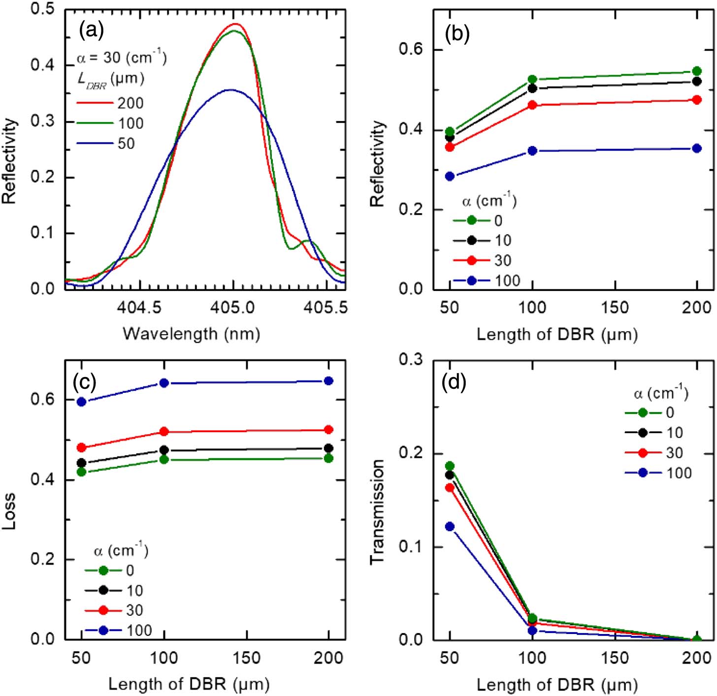
Figure 1.(a) Reflection spectrum for
3. EXPERIMENTS
The group-III nitride laser heterostructure was grown on GaN (0001) substrates using metalorganic vapor phase epitaxy. The p-type Mg-doped layers were activated by annealing the wafers in oxygen-containing ambient. Except for the surface gratings, i-line stepper lithography was used throughout the chip processing. A 2 μm wide and high ridge was fabricated along the whole 600 μm long chip using plasma etching. As shown in Fig. 2(a), the ridge consists of an unpumped DBR section and a pumped gain section. The ratio of the corresponding lengths has been varied as follows: 50/550, 100/500, and 200/400 (length in μm). 1.5 μm wide Pd/Pt p-contact stripes were fabricated on the gain section only. Tenth-order surface gratings with 802 nm period were written on the DBR section of the ridge with 0.25 μm distance from its edges employing electron-beam lithography and plasma etching as shown in Fig. 2(b). The grooves have an opening width at the surface of , a depth of , a slant angle of 20°, and a tip width of [see Fig. 2(c)]. The DBR section was passivated using 300 nm thick . The rest of the chip process followed standard procedures. The laser chips were provided with an antireflection coating () on the rear facet (DBR section) and a low-reflection coating () on the front facet (gain section). They were soldered p-side up on CuW submounts again soldered on Ni/Au-plated copper heat sinks, so called C-mounts. All measurements were performed under CW operation in normal laboratory atmosphere. The light output power and voltage versus current () characteristics of the laser diodes from the rear and front facets were measured, keeping the C-mount temperature at 20°C. High-resolution emission spectra at variable temperature and current were measured with an optical spectrum analyzer (Yokogawa AQ6373), providing a resolution limit of 0.02 nm.
![]()
Figure 2.(a) Schematic side view of a DBR laser diode consisting of a gain section and a DBR section; top-view scanning electron microscope images of (b) the DBR laser chip before the
4. RESULTS
Figure 3 shows the characteristics of the DBR laser diodes of different with the power measured from both facets. It should be mentioned that the lasers were not burned in before the measurement and, during the initial CW operation especially, the bias changes slightly. This explains the differences between the I-V curves in Figs. 3(a) and 3(b). Changes in optical power due to burn-in effects or degradation are small compared to the differences between lasers with DBR gratings of different lengths discussed below. The threshold current of the DBR laser diodes does not significantly depend on and is in the range . The average threshold current density (threshold current over ridge area) and the average slope efficiency of several nominally identical DBR laser diodes were determined to be and , respectively, for ; and , respectively, for ; and and , respectively, for . The increased average threshold current density with increasing and hence decreasing could be attributed to enhanced mirror losses , given by
![]()
Figure 3.Optical power-current-voltage characteristics of DBR laser diodes with
Here, is the constant chip length, is the reflectivity of the front facet, and is the reflectivity of the DBR section. The observed laser output power jump at the threshold indicates the presence of a saturable absorber in the unpumped DBR section, which results in a hysteresis and bistable laser behavior. Based on simulations, a DBR section longer than 50 μm should provide a mode reflectivity larger than 0.28 (when the modal absorption is lower than ), which is independent of the DBR section length. Therefore, increasing the DBR section length () would be equivalent to reducing the effective resonator length alone, and the slope efficiency at the front facet should increase. This fits the experimental data. However, the ratios of output powers from the rear facet and the front facet () measured at 30% above threshold of the DBR laser diodes with the of 50, 100, and 200 μm were 1.23, 0.62, and 0.13, respectively. The continued decrease of , even for large values of , is unexpected. Furthermore, the DBR laser diode with of 50 μm showed multi-peak emission (not shown here). This suggests that the 50 μm long DBR section does not operate as a wavelength-selective mirror as intended and that its reflectivity is lower than that of the front facet (). Moreover, both the 100 μm long and 200 μm long DBR sections showed higher rear facet emission than expected by simulations. Similarly unexpected is the fact that the 100 μm long DBR section shows an around 5 times higher than the 200 μm long DBR section. The differences between simulation and experiment could result from structural imperfections of the fabricated gratings, which are associated with optical losses, or from simplifications of the grating structure in simulations. In reality, the grating is not laterally infinitely extended but even somewhat narrower than the ridge. Therefore, the simulations probably overestimate the reflectivity of the grating and underestimate its losses.
DBR laser diodes with showed periodic steps of the output power, indicating mode hops known from other DBR lasers [17–20]. When the current is increased, the output power seems to level off first before finally a mode hop occurs as shown in Fig. 4(a). The effect can be attributed to a change of the difference in temperature and, therefore, in refractive index between the gain section and the DBR section when increasing the current. With increase of the current, the gain section heats up stronger than the DBR section, and the modal gain spectrum shifts to longer wavelengths while the reflectivity spectrum of the grating is rather fixed. Thus, the slope efficiency decreases when the lasing mode is increasingly shifted away from the maximum of the reflectivity spectrum of the DBR section until lasing hops to the adjacent shorter wavelength mode. This is confirmed by an overall redshift of the lasing wavelength with a wavelength tuning coefficient of 0.002 nm/mA, which is interrupted by steps [see Fig. 4(b)]. The step height of about 0.04 nm agrees with the expected spacing of adjacent longitudinal laser modes. In the current ranges between two mode hops, the laser operates in single longitudinal mode with a full width at half-maximum (FWHM) of the emissions peak of 0.03 nm and a side-mode suppression ratio (SMSR) of 40 dB [see the Fig. 4(b) inset].
![]()
Figure 4.(a) Output power-current characteristic and (b) 2D colormap of emission spectra at different currents of a DBR laser diode with
Temperature-dependent measurements show that single longitudinal mode operation is maintained over a temperature range of 20°C to 40°C with a peak shift of 0.019 nm/K as shown in Fig. 5. This is comparable to the temperature sensitivity of GaN-based DFB laser diodes [12]. Since in this experiment the temperatures of the gain section and the DBR section were changed simultaneously, the previously mentioned mode hops did not occur, and the laser operated on the same longitudinal mode for the entire time.
![]()
Figure 5.Temperature dependence of the peak emission wavelength of a DBR laser diode with
5. SUMMARY
Single longitudinal mode CW operation of 405 nm DBR laser diodes has been demonstrated. Tenth-order surface Bragg gratings with V-shaped grooves were defined on 2 μm wide ridges with 0.25 μm distance from the edge of the ridge employing electron-beam lithography and plasma etching. With increasing length of the DBR section, the ratio of output power from the rear facet to that from the front facet reduced from 1.23 to 0.13. Thermal detuning of the gain section and the DBR section with increasing operation current resulted in periodic oscillations of the output power at the front facet due to mode hops. Between the mode hops, single-mode operation at around 405 nm with an FWHM of 0.03 nm (resolution limit of 0.02 nm) and an SMSR of 40 dB was obtained. Temperature-dependent measurements indicated single longitudinal mode operation between 20°C and 40°C and a linear redshift of the lasing wavelength of 0.019 nm/K. This is comparable to the temperature sensitivity of GaN-based DFB lasers.
Acknowledgment
Acknowledgment. The authors thank the process technology department and the mounting and assembly department of Ferdinand-Braun-Institut and, particularly, K. Ickert and K. Kunkel, for their dedicated support in the chip processing.
References
[1] S. Nakamura, S. Pearton, G. Fasol. The Blue laser Diode: The Complete Story, 7(2000).
[2] Y. Shimada, Y. Chida, N. Ohtsubo, T. Aoki, M. Takeuchi, T. Kuga, Y. Torii. A simplified 461-nm laser system using blue laser diodes and a hollow cathode lamp for laser cooling of Sr. Rev. Sci. Instrum., 84, 063101(2013).
[3] O. Kock, W. He, D. Swierad, L. Smith, J. Hughes, K. Bongs, Y. Singh. Laser controlled atom source for optical clocks. Sci. Rep., 6, 37321(2016).
[4] S. Watson, M. Tan, S. P. Najda, P. Perlin, M. Leszczynski, G. Targowski, S. Grzanka, A. E. Kelly. Visible light communications using a directly modulated 422 nm GaN laser diode. Opt. Lett., 38, 3792-3794(2013).
[5] C. Lee, C. Zhang, M. Cantore, R. M. Farrell, S. H. Oh, T. Margalith, J. S. Speck, S. Nakamura, J. E. Bower, S. P. DenBaars. 4 Gbps direct modulation of 450 nm GaN laser for high-speed visible light communication. Opt. Express, 23, 16232-16237(2015).
[6] V. Tronciu, N. Werner, H. Wenzel, H.-J. Wünsche. Feedback sensitivity of detuned DBR semiconductor lasers. IEEE J. Quantum Electron., 57, 2100107(2021).
[7] H. Y. Ryu, K. H. Ha, J. K. Son, S. N. Lee, H. S. Paek, T. Jang, Y. J. Sung, K. S. Kim, H. K. Kim, Y. Park, O. H. Nam. Determination of internal parameters in blue InGaN laser diodes by the measurement of cavity-length dependent characteristics. Appl. Phy. Lett., 93, 011105(2008).
[8] H. Zhang, C.-W. Shih, D. Martin, A. Caut, J.-F. Carlin, R. Butté, N. Grandjean. Short cavity InGaN-based laser diodes with cavity length below 300 μm. Semicond. Sci. Technol., 34, 085005(2019).
[9] J. Cho, S. Cho, B. J. Kim, S. Chae, C. Sone, O. H. Nam, J. W. Lee, Y. Park, T. I. Kim. InGaN/GaN multi-quantum well distributed Bragg reflector laser diode. Appl. Phy. Lett., 76, 1489-1491(2000).
[10] V. Dumitru, H. Schweizer, H. Gräbeldinger, R. Härle, S. Bader, G. Brürderl, A. Weimar, A. Lell, V. Härle. InGaN/GaN multi-quantum well distributed Bragg reflector laser diode with second-order gratings. Electron. Lett., 39, 372-373(2003).
[11] W. Xie, J. Li, M. Liao, Z. Deng, W. Wang, S. Sun. Narrow linewidth distributed Bragg reflectors based on InGaN/GaN laser. Micromachines, 10, 529(2019).
[12] J. H. Kang, M. Martens, H. Wenzel, V. Hoffmann, W. John, S. Einfeldt, T. Wernicke, M. Kneissl. Optically pumped DFB lasers based on GaN using 10th-order laterally coupled surface gratings. IEEE Photon. Technol. Lett., 29, 138-141(2017).
[13] J. H. Kang, H. Wenzel, V. Hoffmann, E. Freier, L. Sulmoni, R.-S. Unger, S. Einfeldt, T. Wernicke, M. Kneissl. 10th order laterally coupled GaN-based DFB laser diodes with V-shaped surface gratings. Proc. SPIE, 10553, 105530A(2018).
[14] J. H. Kang, H. Wenzel, V. Hoffmann, E. Freier, L. Sulmoni, R.-S. Unger, S. Einfeldt, T. Wernicke, M. Kneissl. DFB laser diodes based on GaN using 10th order laterally coupled surface gratings. IEEE Photon. Technol. Lett., 30, 231-234(2018).
[15] J. H. Kang, H. Wenzel, E. Freier, V. Hoffmann, O. Brox, J. Fircke, L. Sulmoni, M. Matalla, C. Stölmacker, M. Kneissl, M. Weyers, S. Einfeldt. Continuous-wave operation of DFB laser diodes based on GaN using 10th-order laterally coupled surface gratings. Opt. Lett., 45, 935-938(2020).
[16] H. Wenzel, R. Guther, A. M. Shams-Zadeh-Amiri, P. Bienstman. A comparative study of higher order Bragg gratings: coupled-mode theory versus mode expansion modeling. IEEE J. Quantum Electron., 42, 64-70(2006).
[17] J. Fricke, H. Wenzel, M. Matalla, A. Klehr, G. Erbert. 980-nm DBR lasers using higher order gratings defined by i-line lithography. Semicond. Sci. Technol., 20, 1149-1152(2005).
[18] M. Radziunas, K.-H. Hasler, B. Sumpf, T. Y. Tien, H. Wenzel. Mode transitions in distributed Bragg reflector semiconductor lasers: experiments, simulations and analysis. J. Phys. B, 44, 105401(2011).
[19] J. S. Major, D. F. Welch. Singlemode InGaAs/GaAs distributed Bragg reflector laser diodes operating at 1083 nm. Electron. Lett., 29, 2121-2122(1993).
[20] V.-M. Korpijärvi, J. Viheriälä, M. Koskinen, A. T. Aho, M. Guina. High-power temperature-stable GaInNAs distributed Bragg reflector laser emitting at 1180 nm. Opt. Lett., 41, 657-660(2016).

Set citation alerts for the article
Please enter your email address
© Copyright 2018-2021 | Chinese Laser Press. All Rights Reserved 沪ICP备15018463号-20