• Journal of Infrared and Millimeter Waves
  • Vol. 40, Issue 3, 285 (2021)
Kai-Hao CHEN1、2, Zhi-Cheng XU1、*, Zhao-Ming LIANG1, Yi-Hong ZHU1, Jian-Xin CHEN1、**, and Li HE1
Author Affiliations
  • 1Key Laboratory of Infrared Imaging Materials and Detectors, Shanghai Institute of Technical Physics, Chinese Academy of Sciences, Shanghai 200083, China
  • 2University of Chinese Academy of Sciences, Beijing 100049, China
  • show less
    DOI: 10.11972/j.issn.1001-9014.2021.03.001 Cite this Article
    Kai-Hao CHEN, Zhi-Cheng XU, Zhao-Ming LIANG, Yi-Hong ZHU, Jian-Xin CHEN, Li HE. Molecular beam epitaxy growth and characteristics of the high quantum efficiency InAs/GaSb type-II superlattices MWIR detector[J]. Journal of Infrared and Millimeter Waves, 2021, 40(3): 285 Copy Citation Text show less
    Eight measurement locations on the 3 inch MWIR detector wafer for uniformity characterization
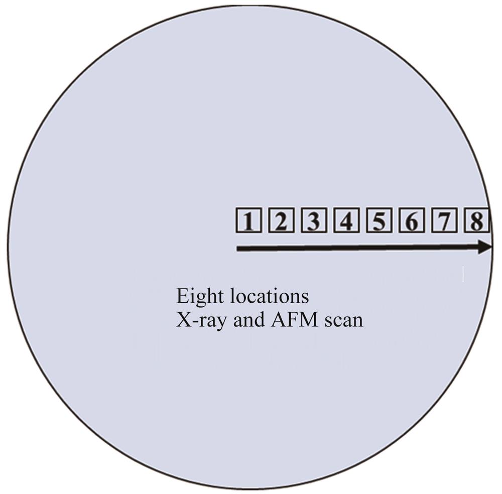
    Fig. 1. Eight measurement locations on the 3 inch MWIR detector wafer for uniformity characterization
    The schematic cross section profile of the MWIR detector structure
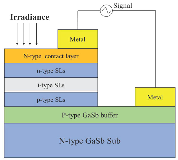
    Fig. 2. The schematic cross section profile of the MWIR detector structure
    The HRXRD ω-2θ scanning curves of eight points along the wafer radius
    Fig. 3. The HRXRD ω-2θ scanning curves of eight points along the wafer radius
    Uniformity results of the(a)lattice mismatch、(b)FWHM and(c)periodic thickness of the MWIR detector along the wafer radius
    Fig. 4. Uniformity results of the(a)lattice mismatch、(b)FWHM and(c)periodic thickness of the MWIR detector along the wafer radius
    The 5 μm × 5 μm AFM images of eight locations along the wafer radius
    Fig. 5. The 5 μm × 5 μm AFM images of eight locations along the wafer radius
    The RMS roughness values of the MWIR detector along the wafer radius
    Fig. 6. The RMS roughness values of the MWIR detector along the wafer radius
    The quantum efficiency spectrum of the P-I-N MWIR detector at 77 K
    Fig. 7. The quantum efficiency spectrum of the P-I-N MWIR detector at 77 K
    The measured(solid line) and fitted(scatter line) dark current density-bias voltage(J-V) curves and dynamic resistance-area product(RA) and voltage(V) curve from a 100 μm×100 μm device
    Fig. 8. The measured(solid line) and fitted(scatter line) dark current density-bias voltage(J-V) curves and dynamic resistance-area product(RA) and voltage(V) curve from a 100 μm×100 μm device
    The Johnson noise limited detectivity of the T2SLs MWIR detector at 77 K
    Fig. 9. The Johnson noise limited detectivity of the T2SLs MWIR detector at 77 K
    Kai-Hao CHEN, Zhi-Cheng XU, Zhao-Ming LIANG, Yi-Hong ZHU, Jian-Xin CHEN, Li HE. Molecular beam epitaxy growth and characteristics of the high quantum efficiency InAs/GaSb type-II superlattices MWIR detector[J]. Journal of Infrared and Millimeter Waves, 2021, 40(3): 285
    Download Citation