Abstract
A very high quantum efficiency InAs/GaSb T2SL mid-wavelength infrared (MWIR) photodetector has been grown by molecular beam epitaxy (MBE). The T2SL detector structure material exhibited smooth surface with step-flow growth and excellent structural homogeneity. The 50% cut-off wavelength was about 5.5 μm. The peak current responsivity was 2.6 A/W corresponding to a quantum efficiency over 80% at 77 K, which was comparable to that of MCT. At 77 K, the dark current density at -50 mV bias was 1.8×10⁻⁶ A/cm2 and the resistance-area product (RA) at maximum (-50 mV bias) was 3.8×10⁵ Ω·cm2. The peak detectivity was calculated to be 6.1 × 1012 cm Hz1/2/W.Introduction
InAs/GaSb type-II superlattice(T2SL) has attracted much attention in the field of infrared detection due to its excellent properties, such as high absorption coefficients comparable to HgCdTe, reduced tunneling currents, suppressed Auger recombination rates, high uniformity and yields based on the robust III-V material system etc. In the past few years, the T2SL’s advantages have been constantly verified[1-4]. Especially with the development of epitaxy and fabrication technologies, large-format and high-performance T2SLs FPAs have been demonstrated[5, 6] in recent years.
Despite the rapid progress, the performances of InAs/GaSb T2SLs detectors have not reached their theoretical predictions yet. The QE of T2SLs detectors is about 30%~50%, while that of MCT detectors is over 80%. One reason is the relatively short carrier lifetime of nearly 30 ns to 100 ns due to the Shockley-Read-Hall recombination, which limits the photo-generated carrier diffusion length[7, 8]. In contrast, the carrier lifetime of MCT can exceed 1μs. Another reason is the insufficient light absorption due to the relatively thin T2SLs epitaxial material. The InSb interfaces have been widely used to achieve the MBE growth of lattice-matched T2SLs. On one hand, we can realize strain compensation with the intentionally inserted interfacial layer [9]. On the other hand, the interfaces can be used to handle the growth transition between adjacent GaSb and InAs layers where there are no common atoms. However, due to a high lattice mismatch of 6% between InSb interfacial layer and InAs or GaSb layer [10-12], the 3D-mode growth happens easily [13, 14]. As a result, the surface morphology and crystalline quality would probably deteriorate as the epitaxial layer thickness increases where commonly contains thousands of interfaces. Therefore, it is a difficult task to grow enough thick T2SLs epitaxial material with good quality, which in turn limits the improvement of T2SLs detectors’ quantum efficiency.
In this paper, we present a high QE T2SLs MWIR detector grown by MBE. Based on a novel MBE shutter sequence, we realized step-flow growth of T2SLs epitaxial materials with smooth surface and excellent structural homogeneity. The total thickness of T2SLs epitaxial layers is 4.4 μm, corresponding to 900 periods. The fabricated detector shows a QE over 80%, comparable to that of MCT. Finally, the opto-electronic properties of the device have been discussed.
1 Experiments
The detector structure material was grown on a 3-inch n-doped(100) GaSb substrate by solid-source molecular beam epitaxy. Valve cracking cells for arsenic and antimony sources are employed to produce dimer As2 and Sb2, respectively. The growth rates were 0.5 ML/s for GaSb and 0.35 ML/s for InAs. An infrared pyrometer was used to measure the growth temperature. The substrate temperature was elevated above 500 ℃ to desorb the surface oxides firstly, and a GaSb buffer layer was grown. Then it was reduced to 400 ℃ for T2SLs growth. A novel MBE growth shutter sequence has been carefully designed to obtain smooth surface. At the GaSb to InAs interface, gallium and antimony source shutters were closed and indium and arsenic source shutters were opened simultaneously. At the InAs to GaSb interface, indium and arsenic shutters were closed firstly, then the antimony source shutter was opened for soaking with several seconds. During the entire epitaxy process, the direct deposition of InSb interface layers has been avoided. By adjusting Sb soaking time, we managed to modulate the lattice mismatch between T2SLs and GaSb substrates.
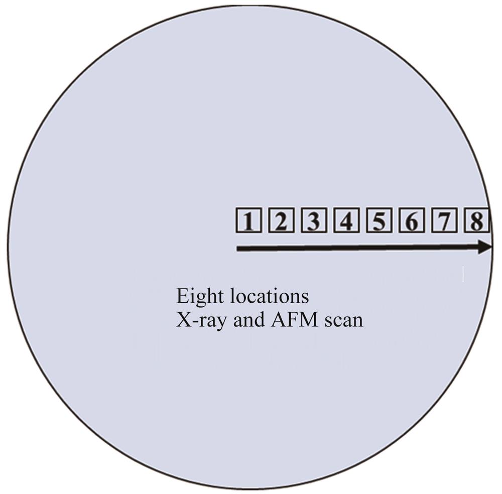
The detector has a P-I-N structure. It consists of 1-μm-thick p-type GaSb layer, 50 periods of p-type doped 9.5 ML InAs/7 ML GaSb, 800 periods of unintentionally doped 9.5 ML InAs/7 ML GaSb SLs absorber region, 50 periods of n-type doped 9.5 ML InAs/7 ML GaSb, and a 30-nm-thick n-type doped InAs layer. The bottom P-GaSb and top N-InAs were served as electrical contact layers. The structural characteristics of the superlattices, such as lattice mismatch and period thickness, were measured by a Panalytical high-resolution X-ray diffraction(HRXRD). The surface morphology was scanned by a Park NX20 atomic force microscope(AFM). Eight locations, 5mm apart from each other along the 3-inch wafer radius were chosen to investigate the uniformity, as shown in Fig. 1.

Figure 1.Eight measurement locations on the 3 inch MWIR detector wafer for uniformity characterization
The P-I-N detector structure material was processed into single element mesas by wet chemical etching, as shown in Fig. 2. Ohmic contacts were made by electron beam deposition of TiPtAu metals. Current-voltage and optical response measurements were performed at liquid nitrogen temperature. The quantum efficiency spectrum was measured by a Fourier transform infrared spectrometer and calibrated with a blackbody at temperature of 800 K. The detector was designed to receive the irradiance from the front side.
Figure 2.The schematic cross section profile of the MWIR detector structure
2 Results and discussions
Figure 3 shows the HRXRD ω-2θ scanning curves along the 3-inch wafer radius. The diffraction curves have clear and sharp satellite peaks, and can be excellently superposed with each other, indicating the high crystalline quality and uniformity. The zero-order diffraction peak of superlattices almost coincides with that of GaSb substrate, which means that the lattice mismatch is nearly zero. All the lattice mismatches along the radius have depicted as shown in Fig. 4(a). The first-order peaks’ full width at half maximum(FWHM) of all XRD curves have been summarized in Fig. 4(b). A FWHM of around 25 arcsec has been achieved, comparable to that of the thinner T2SLs material reported in our previous paper[15]. The periodic thickness of T2SLs was calculated to be around 49 Å from the satellite peaks spacing as shown in Fig. 4(c), which was close to the design thickness(49.5Å), proving the precise MBE growth control. All values of lattice mismatch, FWHM and period thickness along the radius show very small fluctuations.
Figure 3.The HRXRD ω-2θ scanning curves of eight points along the wafer radius
Figure 4.Uniformity results of the(a)lattice mismatch、(b)FWHM and(c)periodic thickness of the MWIR detector along the wafer radius
The AFM images on a 5 μm × 5 μm scan area along the wafer radius are shown in Fig. 5. All scans exhibit similar surface morphology with clear atomic steps, demonstrating a step-flow growth mode. The root mean square(RMS) roughness values are presented in Fig. 6, maintaining a relatively low level of about 0.2 nm. The two-dimensional layer by layer growth of T2SLs epitaxial layers has made it easier to prepare thicker materials with high uniformity.
Figure 5.The 5 μm × 5 μm AFM images of eight locations along the wafer radius
Figure 6.The RMS roughness values of the MWIR detector along the wafer radius
Figure 7 shows the quantum efficiency spectrum of the processed mid-wavelength detector at 77 K. The 100% cut-off wavelength is about 6 μm. The peak current responsivity is 2.6 A/W at 4.6 μm, corresponding to a quantum efficiency over 80%, which is the best of the ever reported T2SL detectors[16-19]. The reflection loss at the photodiode surface is not considered here. The bias dependence of peak current responsivity for the photodetector is also shown in the inset of Fig. 7. The photo-response is fully turned on at zero bias, which implies the photo-generated carrier has a diffusion length longer than the absorption region.
Figure 7.The quantum efficiency spectrum of the P-I-N MWIR detector at 77 K
The measured dark current density-bias voltage(J-V) curve and its associated dynamic resistance-area product(RA) and voltage(V) curve at 77 K from a 100 μm × 100 μm single element device are shown in Fig. 8. The dark current density at -50mV bias is 1.8×10⁻⁶ A/cm2 and resistance-area product(R0A) at zero bias is 1.2×10⁴ Ω·cm2. To explore the electrical properties further, the dark current fitting has been carried out as shown in Fig. 8. Four leakage current sources have been considered including surface(J-sh), generation-recombination(J-gr), diffusion(J-diff) and trap-assisted tunneling currents(J-tat)[20, 21]. It is clear that the dark current mainly derived from the J-sh in the entire bias range. Surface resistance of 2.2×10⁸ Ω has been obtained through the fitting. This reminds us that the thick epitaxial layer would possibly increase the difficulty of device fabrication, especially surface leakage current suppression. Here, it has to be noted that the detectors’ dark current still has a certain gap with the best results reported in ref[22, 23], because a homojunction detector structure is just used in this work. The relatively high generation-recombination current can be observed in Fig. 8 due to the short Shockley-Read-Hall recombination lifetime for a T2SLs detector. The heterojunction detection structure design has to be adopted to reduce T2SLs detectors’ bulk currents further. Figure 9 shows the detector’s Johnson noise limited detectivity spectrum[15]. A peak detectivity of 6.1 x 1012 cm Hz1/2/W has been realized.
Figure 8.The measured(solid line) and fitted(scatter line) dark current density-bias voltage(J-V) curves and dynamic resistance-area product(RA) and voltage(V) curve from a 100 μm×100 μm device
Figure 9.The Johnson noise limited detectivity of the T2SLs MWIR detector at 77 K
3 Conclusions
In summary, it is very important for a T2SLs detector to grow enough thick epitaxial layers to achieve the sufficient absorption of light and high QE. To avoid the island structure, a novel MBE growth shutter sequence has been proposed. Based on the novel shutter sequence, we realize the layer by layer growth of T2SLs epitaxial materials with the smooth surface. A high QE of over 80% P-I-N MWIR infrared detector has been fabricated.
References
[1] D L Smith, C Mailhiot. PROPOSAL FOR STRAINED TYPE-II SUPERLATTICE INFRARED DETECTORS. Journal of Applied Physics, 62, 2545-2548(1987).
[2] A Rogalski. Material considerations for third generation infrared photon detectors. Infrared Physics & Technology, 50, 240-252(2007).
[3] E R Youngdale, J R Meyer, C A Hoffman et al. Auger lifetime enhancement in inas-ga1-xinxsb superlattices. Applied Physics Letters, 64, 3160-3162(1994).
[4] GunapalaS D, TingD Z, HillC J, et al. Conference on Infrared Remote Sensing and Instrumentation XVIII, 2010,7808.
[5] TingD Z, SoibelA, KhoshakhlaghA, et al. Conference on Infrared Technology and Applications XLIII, 2017,10177.
[6] A Williams, M Tidrow. III-V infrared focal plane array development in US (Conference Presentation)(2018).
[7] B C Connelly, G D Metcalfe, H E Shen et al. Direct minority carrier lifetime measurements and recombination mechanisms in long-wave infrared type II superlattices using time-resolved photoluminescence. Applied Physics Letters, 97, 3(2010).
[8] D Donetsky, G Belenky, S Svensson et al. Minority carrier lifetime in type-2 InAs-GaSb strained-layer superlattices and bulk HgCdTe materials. Applied Physics Letters, 97, 3(2010).
[9] J B Rodriguez, P Christol, L Cerutti et al. MBE growth and characterization of type-II InAs/GaSb superlattices for mid-infrared detection. Journal of Crystal Growth, 274, 6-13(2005).
[10] Y Horikoshi. MIGRATION-ENHANCED EPITAXY OF GAAS AND ALGAAS. Semiconductor Science and Technology, 8, 1032-1051(1993).
[11] Y Wei, W Q Ma, Y H Zhang et al. High Structural Quality of Type II InAs/GaSb Superlattices for Very Long Wavelength Infrared Detection by Interface Control. Ieee Journal of Quantum Electronics, 48, 512-515(2012).
[12] Y H Zhang, W Q Ma, Y L Cao et al. Long Wavelength Infrared InAs/GaSb Superlattice Photodetectors with InSb-Like and Mixed Interfaces. Ieee Journal of Quantum Electronics, 47, 1475-1479(2011).
[13] Z Xu, J Chen, F Wang et al. Interface layer control and optimization of InAs/GaSb type-II superlattices grown by molecular beam epitaxy. Journal of Crystal Growth, 386, 220-225(2014).
[14] H J Haugan, G J Brown, L Grazulis. Effect of interfacial formation on the properties of very long wavelength infrared InAs/GaSb superlattices. Journal of Vacuum Science & Technology B, 29, 5(2011).
[15] Z Xu, J Chen, F Wang et al. High quality mid-wavelength infrared InAs/GaSb superlattices by exploring the optimum molecular beam epitaxy growth process. Infrared Physics & Technology, 67, 8-13(2014).
[16] M Huang, J X Chen, Y Zhou et al. Light-harvesting for high quantum efficiency in InAs-based InAs/GaAsSb type-II superlattices long wavelength infrared photodetectors. Applied Physics Letters, 114, 5(2019).
[17] A Haddadi, G Chen, R Chevalier et al. InAs/InAs1-xSbx type-II superlattices for high performance long wavelength infrared detection. Applied Physics Letters, 105, 4(2014).
[18] RehmR, WaltherM, SchmitzJ, et al. Conference on Quantum Sensing and Nanophotonic Devices VI, 2009,7222.
[19] G Chen, A M Hoang, S Bogdanov et al. Effect of sidewall surface recombination on the quantum efficiency in a Y2O3 passivated gated type-II InAs/GaSb long-infrared photodetector array. Applied Physics Letters, 103, 4(2013).
[20] V Gopal, E Plis, J B Rodriguez et al. Modeling of electrical characteristics of midwave type II InAs/GaSb strain layer superlattice diodes. Journal of Applied Physics, 104, 6(2008).
[21] J Nguyen, D Z Ting, C J Hill et al. Dark current analysis of InAs/GaSb superlattices at low temperatures. Infrared Physics & Technology, 52, 317-321(2009).
[22] A Rogalski, P Martyniuk, M Kopytko. Type-II superlattice photodetectors versus HgCdTe photodiodes. Progress in Quantum Electronics, 68, 19(2019).
[23] B Nguyen, P-Y Delaunay, E Huang et al. State-of-the-art Type II antimonide-based superlattice photodiodes for infrared detection and imaging. Proc SPIE(2009).