
A. Pandey, W. J. Shin, J. Gim, R. Hovden, Z. Mi. High-efficiency AlGaN/GaN/AlGaN tunnel junction ultraviolet light-emitting diodes[J]. Photonics Research, 2020, 8(3): 331
- Photonics Research
- Vol. 8, Issue 3, 331 (2020)
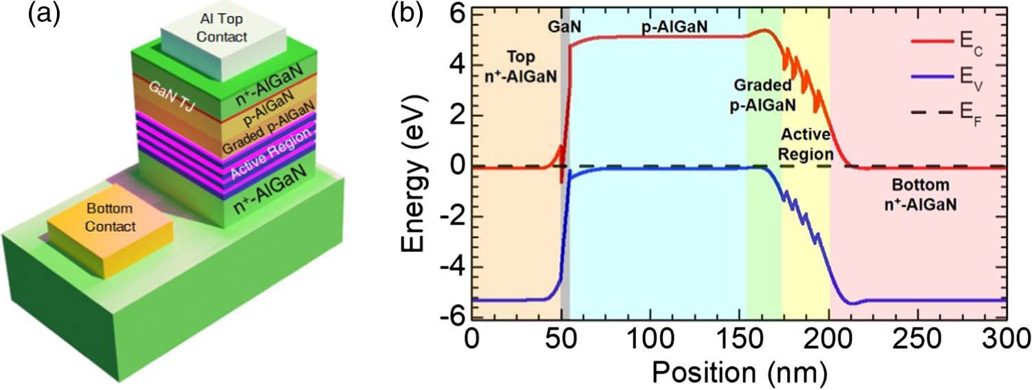
Fig. 1. (a) Schematic illustration of the tunnel junction LED structures. (b) Simulated equilibrium band diagram for a representative LED using a 5 nm GaN layer within the tunnel junction. The different layers used in the structure are labelled and shown with different colors.
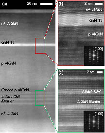
Fig. 2. (a) HAADF-STEM overview of cross-sectional AlGaN multilayers shows the complete device structure consistent with the device design. (b) High-resolution HAADF-STEM of the p-AlGaN/GaN/n-AlGaN tunnel junction shows crystalline epitaxial growth with sharp interfaces for enhanced hole injection by tunneling. (c) Atomic-resolution HAADF-STEM of Al 0.6 Ga 0.4 N Al 0.85 Ga 0.15 N
Fig. 3. (a) I –V characteristics of tunnel junction LED Samples A and B, with 2.5 nm GaN layer width and different thicknesses, 50 and 150 nm respectively, of top n + I –V characteristics of Samples B, C, and D grown with the same thickness of top n +
Fig. 4. I –V characteristics of an optimized tunnel junction LED from Sample E with a GaN layer thickness of 5 nm and top n ∼ 480 nm
Fig. 5. (a) Electroluminescence spectra measured at different injection currents for a representative tunnel junction LED. Inset shows an electroluminescence spectrum measured at 25 A / cm 2
Fig. 6. Variations of (a) EQE and (b) WPE with injected current density for an LED from Sample E.
|
Table 1. Parameters of Tunnel Junction LED Structures

Set citation alerts for the article
Please enter your email address
© Copyright 2018-2021 | Chinese Laser Press. All Rights Reserved 沪ICP备15018463号-20