A. Pandey, W. J. Shin, J. Gim, R. Hovden, Z. Mi, "High-efficiency AlGaN/GaN/AlGaN tunnel junction ultraviolet light-emitting diodes," Photonics Res. 8, 331 (2020)
Copy Citation Text
AlGaN is the material of choice for high-efficiency deep UV light sources, which is the only alternative technology to replace mercury lamps for water purification and disinfection. At present, however, AlGaN-based mid- and deep UV LEDs exhibit very low efficiency. Here, we report a detailed investigation of the epitaxy and characterization of LEDs utilizing an AlGaN/GaN/AlGaN tunnel junction structure, operating at ~, which have the potential to break the efficiency bottleneck of deep UV photonics. A thin GaN layer was incorporated between and -AlGaN to reduce the tunneling barrier. By optimizing the thickness of the GaN layer and thickness of the top -AlGaN contact layer, we demonstrate AlGaN deep UV LEDs with a maximum external quantum efficiency of 11% and wall-plug efficiency of 7.6% for direct on-wafer measurement. It is also observed that the devices exhibit severe efficiency droop under low current densities, which is explained by the low hole mobility, due to the hole hopping conduction in the Mg impurity band and the resulting electron overflow.
Video Introduction to the Article
1. INTRODUCTION
According to the World Health Organization, health-care-associated infections (HCAIs) [1] and water-borne illnesses [2] are responsible for thousands of fatalities and billions of dollars in costs each year. Sterilization of medical equipment and water supplies is now frequently utilized to minimize the possibility of infections by neutralizing pathogens; for this purpose, conventional mercury ultraviolet (UV) lamps have been widely used. Semiconductor optoelectronic devices offer an alternative that is nontoxic, more compact, and more flexible in applications. The AlGaN alloy system is uniquely suited for this purpose, as the alloys are direct bandgap semiconductors spanning from to in wavelengths. To date, AlGaN light-emitting diodes (LEDs) operating in the UV-C band (200–280 nm), which is of prime importance for sterilization, exhibit low efficiency, which has been attributed to the poor light extraction associated with transverse magnetic (TM)-polarized light emission [3–6], low luminescence efficiency due to the presence of large densities of defects [7,8], and inefficient -type doping [9–11]. These issues become more severe for LEDs operating at shorter wavelengths, which require higher Al content in the device active region. In this regard, intensive studies have been performed to improve the light-extraction efficiency by engineering the energy band structure [12,13] and by utilizing nanostructures [14–17]. Various techniques, including epitaxy on nanopatterned substrates and high-temperature annealing, have also been developed to reduce the formation of defects [18–21]. Recently, external quantum efficiency (EQE) over 20% was reported for AlGaN LEDs operating at 275 nm, which, however, had a low wall-plug efficiency (WPE) of 5.7% [22]. To our knowledge, the best reported EQE for AlGaN LEDs operating at , an important wavelength for water purification and sterilization [23], is for packaged devices grown using metal–organic chemical vapor deposition (MOCVD) [24,25]. Direct on-wafer measurements, however, typically result in lower efficiencies due to reduced light extraction/collection and severe self-heating of the devices, with the best peak EQE of only at [26,27]. The maximum wall-plug efficiency of these devices is often much lower, which is fundamentally limited by the large resistance and poor hole injection efficiency, due to the high resistivity of -type AlGaN. Moreover, the poor -type conduction, together with the highly asymmetric hole and electron injection efficiencies, can lead to parasitic carrier recombination outside the active region [28,29], which further exacerbates the heating of the devices and can have a detrimental impact on device performance [30–33]. While using -GaN as the contact layer may partly alleviate the issue of hole injection to the active region, it has an adverse impact on light extraction efficiency, due to the significant UV light absorption by GaN [34].
A promising technique to improve hole injection is through the use of a tunnel junction structure, wherein holes are injected into the valence band of the -type layer by the interband tunneling of electrons to the conduction band of an -type layer. Using the tunnel junction structure, the high resistance -AlGaN layer can be replaced by a relatively low resistance -AlGaN contact layer, which further allows the use of a reflective Al ohmic contact to enhance the light extraction for backside emitting devices [35–37]. Homojunction tunnel diodes in the III-nitrides have been previously demonstrated using highly doped GaN [38–40]; however, the doping required for efficient interband tunneling of carriers becomes extremely difficult to attain in AlGaN alloys due to their higher bandgaps and less efficient -type doping. Such critical challenges can be addressed, to a certain extent, through polarization engineering by incorporating a thin layer of different composition between the - and -type layers [41–44]. Due to the strong spontaneous and piezoelectric polarization, the sheet charges at the hetero interfaces help to better align the conduction band of the -type layer with the valence band of the -type layer, while reducing the width of the depletion region. This results in a dramatic increase in the probability of electron tunneling. Such a technique has been employed in visible LEDs [45] and lasers [46] and has also been demonstrated using an InGaN-based tunnel junction for UV LEDs grown using molecular beam epitaxy (MBE) [36,47,48] and GaN-based tunnel junction for UV LEDs grown using MOCVD [49].
In this work, we demonstrate the use of a GaN polarization engineered tunnel junction with a -AlGaN/GaN/n-AlGaN structure, to realize high-efficiency AlGaN LEDs operating at 265 nm. A series of samples with different GaN widths and thicknesses of the top -AlGaN contact layer were grown and fabricated, and their effect on device performance was thoroughly studied. Through detailed optimization, we demonstrate LEDs having emission wavelengths with a maximum EQE of 11%. The peak WPE was measured to be 7.6%. It is also observed that these devices exhibit severe efficiency droop at relatively low current densities. The underlying causes have been discussed. This work provides new insights into the performance improvement of AlGaN deep UV LEDs.
Sign up for Photonics Research TOC. Get the latest issue of Photonics Research delivered right to you!Sign up now
2. EPITAXIAL GROWTH OF LEDS
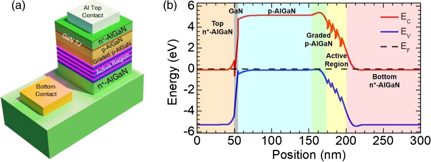
The tunnel junction LED structures were grown in a Veeco Gen 930 plasma-assisted molecular beam epitaxy (PA-MBE) system on 1 μm thick AlN-on-sapphire substrates from DOWA Holdings Co., Ltd. A nitrogen flow rate of 0.6 sccm (standard cubic centimeters per minute), with an RF power of 350 W was used throughout the growth. The growth rate is for the AlGaN epilayers. The growth was conducted using metal-semiconductor junction-assisted epitaxy to enhance Mg-dopant incorporation and to reduce defect formation [50]. A schematic of the LED structures is shown in Fig. 1(a). The growth was initiated with a thick AlN layer, followed by the subsequent AlGaN growth. The initial thick layer was Si-doped to form the bottom -contact. The Al composition of the AlGaN was graded up from 65% to 85% in a thickness of immediately before the active region. The active region consisted of four AlGaN quantum wells with compositions designed for peak emission at . The AlGaN barriers, with higher Al compositions, were grown with decreasing thicknesses, from to closer to the Mg-doped AlGaN. A graded Mg-doped AlGaN layer, with a thickness of and Al compositions varying from 80% to 65%, followed the last quantum well. The grading down of the Al composition of the AlGaN provides polarization-induced doping, which enhances the hole concentration [51]. A thick was then grown, followed by the GaN layer. Compared with the previously reported InGaN-based tunnel junction UV LEDs grown by MBE [36,37,47,48,52], there was no growth interruption for the tunnel junction, as the substrate temperature was kept the same as that for the GaN and AlGaN layers. Following the growth of the tunnel junction, the top contact layer was grown. Different design parameters, including the thicknesses of the GaN layer and the top -AlGaN contact layer, are listed in Table 1. A 1D Poisson-Schrödinger solver was used to simulate the band diagram of a representative structure having 5 nm GaN width, as shown in Fig. 1(b).
Figure 1.(a) Schematic illustration of the tunnel junction LED structures. (b) Simulated equilibrium band diagram for a representative LED using a 5 nm GaN layer within the tunnel junction. The different layers used in the structure are labelled and shown with different colors.
High-angle annular dark field scanning transmission electron microscopy (HAADF-STEM) on a representative sample confirms the AlGaN multilayer structure with tunnel junction and AlGaN quantum well layers, as shown in Fig. 2(a). The GaN layer () is epitaxially grown between the top -AlGaN contact and -AlGaN layer with sharp interfaces, as shown in Fig. 2(b). The ratio of HAADF STEM intensity estimates less Ga in the -AlGaN layers compared with the Ga concentration in the GaN layer. The high relative Ga content in the tunnel junction is expected to increase the efficiency of charge carrier injection by tunneling. High-resolution cross-sectional STEM, as shown in Fig. 2(c), also confirms the epitaxial growth of four AlGaN quantum wells () with higher content of Ga relative to adjacent AlGaN barriers (ranging from to ) that confine charge carriers. Fast Fourier transform (FFT) of the atomic resolution HAADF STEM images confirms the (100) lattice plane of AlGaN multilayers with an orientation that indicates preferred growth along the [001] -axis direction. Relative gallium concentration in GaN tunnel junction and AlGaN quantum well/barrier layers was formulated by the HAADF intensity along [100] defined by where is the high-angle annular dark field intensity, is the cross-section thickness, is the concentration of Ga or Al in the AlGaN multilayers, is the atomic number of Al, Ga, or N in the layers, and is between 1.4 and 1.7. HAADF-STEM was collected using a Cs aberration corrected JEOL 3100R05 microscope (300 keV, 22 mrad) and a 120 mm camera length.
Figure 2.(a) HAADF-STEM overview of cross-sectional AlGaN multilayers shows the complete device structure consistent with the device design. (b) High-resolution HAADF-STEM of the p-AlGaN/GaN/n-AlGaN tunnel junction shows crystalline epitaxial growth with sharp interfaces for enhanced hole injection by tunneling. (c) Atomic-resolution HAADF-STEM of quantum wells coupled to barriers with sharp epitaxial interfaces for carrier confinement.
All 265 nm LED structures were fabricated using the same process to maximize emission from the backside of the wafer. A plasma was first used to dry-etch the samples down to the bottom -contact layer, with device mesas having an area size of μμ. This was followed by the deposition of a dielectric distributed Bragg reflector (DBR) to increase light reflection toward the backside of the wafer and also serve as a surface passivation layer. The thicknesses of and layers are and , respectively, which were calculated based on the measured refractive indices of the dielectric layers and an epilayer, to maximize reflectivity around 265 nm. Openings were then etched into the passivation layer for the deposition of metal contacts. A reflective top contact of Al (250 nm)/Au (50 nm) was then deposited [35,37], followed by a Ti (40 nm)/Al (120 nm)/Ni (40 nm)/Au (50 nm) metal stack for the bottom -contact. The metal contacts were annealed at 700°C for 30 s in nitrogen ambient.
Measurements were performed using an AV-1010B pulse generator, with a 1% duty cycle and a 10 kHz repetition rate to minimize heating effect. A calibrated Newport 818-ST2-UV silicon photodetector with a Newport Model 1919-R power meter was used to measure the device output power. Shown in Fig. 3(a) are the current–voltage characteristics for Samples A and B, which have a 2.5 nm thick GaN layer between the highly doped AlGaN layers, but with different thicknesses of the top -AlGaN contact layer. It is seen that the devices exhibit similar I–V characteristics under relatively low current densities. Higher current densities, however, can only be measured in Sample B, which has a thicker () top -AlGaN contact layer. Slightly higher efficiency was also measured for Sample B, compared with Sample A. We have subsequently studied the effect of different thicknesses of the GaN layer within the tunnel junction on the device efficiency, while keeping the top -AlGaN contact layer thickness at 150 nm. The GaN layer thicknesses were varied from 2.5 nm (Sample B), 5 nm (Sample C), to 10 nm (Sample D). I–V characteristics of these devices were measured and are shown in Fig. 3(b). It is seen that Samples C and D have slightly better turn-on voltage, compared with Sample B. The small difference between the turn-on voltages of the different structures indicates that tunneling through the tunnel junction might be dominated by trap-assisted tunneling [53,54]. Studies on AlGaN/GaN-based double-barrier resonant tunnel diodes have suggested that trapped charges at the hetero-interface are responsible for the observed electrical characteristics [55]. It has also been shown previously that a high concentration of impurity atoms at the tunnel junction interface can improve the turn-on voltage of the tunnel junction by providing states enabling trap-assisted tunneling [56–58]. The reduced turn-on voltage through trap-assisted tunneling improves the wall-plug efficiency of the tunnel junction LEDs by facilitating carrier transport even at low biases. The measured EQE and WPE are further shown in Figs. 3(c) and 3(d), respectively. A maximum EQE 9.8% was measured for Sample C, whereas maximum EQEs 7.4% and 6.2% were measured for Samples B and D, respectively, suggesting that a GaN layer thickness is optimum for the presented tunnel junction structures. This could be due to the degraded material quality with the incorporation of a thicker GaN layer, whereas a thinner GaN layer may not provide sufficiently strong polarization. Moreover, a thicker GaN layer also increases the absorption of UV light emission from the device’s active region. A thick GaN layer would also present an obstacle to carrier transport due to the increased distance that electrons would need to tunnel across. A peak WPE of 6.9% was measured for Sample C, as shown in Fig. 3(d).
Figure 3.(a) I–V characteristics of tunnel junction LED Samples A and B, with 2.5 nm GaN layer width and different thicknesses, 50 and 150 nm respectively, of top -AlGaN contact layer. (b) I–V characteristics of Samples B, C, and D grown with the same thickness of top -AlGaN but different GaN layer widths of 2.5, 5, and 10 nm, respectively. Variations of (c) EQE and (d) WPE with injected current density, for Samples B, C, and D.
It is interesting to note that all the devices demonstrated a strong droop even at a relatively low current injection of , suggesting that the cause of the droop is independent of the tunnel junction designs. Efficiency droop has been commonly measured for InGaN-based blue and green LEDs at current densities [59,60]. Theunderlying causes for the efficiency droop, including carrier delocalization, Shockley–Read–Hall recombination, Auger recombination, and device heating, have been intensively studied [60–62]. At low current densities of , device heating and Auger recombination are not expected to be significant. As studied previously, the operation of GaN-based LEDs may deviate from low-level injection conditions even under relatively low current densities, due to the asymmetric charge carrier transport [28,63,64]. Due to the large activation energy for Mg dopant in Al-rich AlGaN, -type conduction is primarily mediated by hole hopping in the Mg impurity band at room temperature, which has low mobility [50,65]. For Al-rich AlGaN, the electron mobility is typically on the order of [66], whereas the hole mobility is [67], or lower, while the corresponding maximum electron and hole concentrations are and , respectively. The resulting conductivity of the - and -AlGaN layers is nearly three orders of magnitude different. As a consequence, even at a small current density of , the device operates in a regime that severely deviates from the low-carrier injection condition. The resulting electric field in the p-AlGaN layer, even at a seemingly small current density, affects the transport of holes more severely than that of electrons, due to the large difference in their mobility values. This leads to a significant increase in charge carrier recombination outside of the device active region, i.e., electron overflow to the -AlGaN layer, at a small injection current. A similar effect has also been measured in AlGaN nanowire UV-C LEDs [63]. Further, it should also be noted that, as the epitaxial growth of the entire LED structure was performed under slightly Ga-rich conditions, it is expected that the distribution of Ga may not be uniform in the epilayers [27,68–70]. It has been shown that these Ga-rich regions act as highly efficient radiative recombination sites due to their ability to locally confine excitons. However, as the injected current into the device increases, carrier delocalization will occur, allowing carriers to recombine at nonradiative recombination centers, also resulting in a decrease of device efficiency.
Based on the studies above, a 265 nm deep UV-LED structure with a 5 nm thick GaN layer in the tunnel junction and thick top -AlGaN contact layer (Sample E) was grown and fabricated. The measured current-voltage characteristics are shown in Fig. 4. A large current density of was measured at 16 V, which is significantly better than that measured in Samples A–D as well as tunnel junction UV-C LEDs reported previously having emission at a similar wavelength [37,49]. The high current density measured for this sample suggests that optimization of the tunnel junction by adjusting the width of the GaN layer together with a relatively thick -AlGaN top contact layer, can significantly enhance the current injection and stability of deep UV LEDs.
Figure 4.I–V characteristics of an optimized tunnel junction LED from Sample E with a GaN layer thickness of 5 nm and top -AlGaN contact layer thickness .
Shown in Fig. 5(a) are the electroluminescence spectra of an LED from Sample E measured at different current densities. The spectra were measured using CW bias supplied by a Keithley 2400 SMU, collected using an optical fiber coupled to a high-resolution spectrometer and detected by a charge coupled device. Variations of the peak position and spectral linewidth with current density are shown in Fig. 5(b). It is seen that the device first exhibits a small blueshift from to with increasing current density, followed by a redshift at relatively high injection conditions. The blueshift can be explained by the quantum-confined Stark effect. The polarization field in AlGaN quantum wells is estimated to be based on the shift experimentally observed, assuming that an injected current density of completely flattens the bands in the quantum well, while not significantly affecting the emission wavelengths due to heating. This is substantially less than the predicted theoretical value of 1.5–2.5 MV/cm [71,72], indicating the compensation of the sheet charge by impurities or defects and some degree of relaxation in the AlGaN layers. The redshift at higher operating currents is likely due to heating effect. Such a redshift has also been reported previously for both AlGaN [30] and InGaN [73] LEDs. The spectral linewidths stay nearly constant at at low current densities and broaden to at relatively high injection conditions. It is also noticed that no significant defect-related emission was measured in the UV-C LEDs, as shown in the inset of Fig. 5(a).
Figure 5.(a) Electroluminescence spectra measured at different injection currents for a representative tunnel junction LED. Inset shows an electroluminescence spectrum measured at current density with the intensity in log scale. (b) Variations of peak position (red circles) and spectral linewidth (black squares) versus injected current density.
The measured EQE and WPE of the LED from Sample E are shown in Figs. 6(a) and 6(b), respectively. A maximum EQE of 11% and WPE of 7.6% were measured. The EQE measured here is higher than that of comparable UV LEDs having emission at this wavelength [24–27,48,49], although still below the highest reported for LEDs at 275 nm [22]; however, the tunnel junction devices studied here have a higher WPE due to the more efficient carrier injection from such a structure, which also results in significantly lower turn-on voltages. It is also noticed that, despite the optimization in the tunnel junction structure design, efficiency droop is present at low current injection. The external quantum efficiency of such a diode was fitted using the standard ABC model [74,75]. From the fitted curve (not shown), A, B and C parameter values of , , and were derived. The estimated C value of is around three orders of magnitude higher than the previously reported Auger coefficient of for AlGaN quantum well heterostructures [76], which, together with the presence of efficiency droop at very low current densities (), strongly suggests that other carrier loss mechanisms, such as electron overflow, other than Auger recombination, are the main cause for the efficiency droop of deep UV LEDs [28,63].
Figure 6.Variations of (a) EQE and (b) WPE with injected current density for an LED from Sample E.
In summary, we have studied the design, epitaxy, fabrication, and performance characteristics of tunnel injected deep UV LEDs operating at . Significantly improved current–voltage characteristics and efficiency were measured with the incorporation of GaN layer thickness . The optimized AlGaN deep UV LED exhibited a maximum EQE and WPE of 11% and 7.6%, respectively. The device performance, however, suffers from efficiency droop even at relatively low current densities . The underlying cause is not likely due to Auger recombination but, instead, could be related to electron overflow due to the small hole mobility associated with hole hopping conduction in the Mg impurity band of Al-rich AlGaN. To achieve high efficiency and high-power UV-C LEDs, it is therefore important to improve the hole mobility and -type conduction of AlGaN by improving the epitaxy conditions, heterostructure design, and/or developing new -type wide-bandgap semiconductors.
Acknowledgment
Acknowledgment. The devices were fabricated in the Lurie Nanofabrication Facility at the University of Michigan. The authors acknowledge the Michigan Center for Materials Characterization for electron microscopy.
References
[1] World Health. Guidelines approved by the Guidelines Review Committee. Global Guidelines for the Prevention of Surgical Site Infection(2018).
[2] World Health. Guidelines approved by the Guidelines Review Committee. Guidelines for Drinking-Water Quality(2017).
A. Pandey, W. J. Shin, J. Gim, R. Hovden, Z. Mi, "High-efficiency AlGaN/GaN/AlGaN tunnel junction ultraviolet light-emitting diodes," Photonics Res. 8, 331 (2020)