• Photonics Research
  • Vol. 8, Issue 6, 788 (2020)
Brian Julsgaard1、*, Nils von den Driesch2、3, Peter Tidemand-Lichtenberg4, Christian Pedersen4, Zoran Ikonic5, and Dan Buca2
Author Affiliations
  • 1Department of Physics and Astronomy, Aarhus University, Ny Munkegade 120, DK-8000 Aarhus C, Denmark
  • 2Peter Grünberg Institute 9 (PGI 9), Forschungszentrum Jülich, 52425 Jülich, Germany
  • 3JARA-Institut Green IT, RWTH Aachen, Germany
  • 4DTU Fotonik, Technical University of Denmark, Frederiksborgvej 399, DK-4000 Roskilde, Denmark
  • 5Pollard Institute, School of Electronic and Electrical Engineering, University of Leeds, Leeds, UK
  • show less
    DOI: 10.1364/PRJ.385096 Cite this Article Set citation alerts
    Brian Julsgaard, Nils von den Driesch, Peter Tidemand-Lichtenberg, Christian Pedersen, Zoran Ikonic, Dan Buca. Carrier lifetime of GeSn measured by spectrally resolved picosecond photoluminescence spectroscopy[J]. Photonics Research, 2020, 8(6): 788 Copy Citation Text show less
    (a) Overview of the detection system. An incoming pulsed laser beam (blue) excites a GeSn sample, and the emitted infrared (IR) light (gray) is directed via flat and parabolic mirrors to an upconverter (UC) module, from which the upconverted light (yellow) goes through a monochromator and eventually reaches an avalanche photodiode (APD). The thermal emission of a SiC glowbar can be detected for calibration purposes. (b) Schematic diagram of the UC module. An intracavity field (green) at 1064 nm is mixed with the incoming IR light in a periodically poled lithium niobate (PPLN) crystal, generating the upconverted light (yellow). (c) Schematic representation of involved photon energy ranges, with the two gray and yellow arrows showing the smallest and largest involved energies of the IR and UC light. (d) Measured emission spectra of the glowbar for six different positions of the PPLN crystal motor stage. (e) Example of a decay curve (red) obtained from the GeSn sample at E=0.51 eV, T=20 K, and Φ=2.1×10¹⁵ photons/cm2. The black curve shows the instrument response function (IRF).
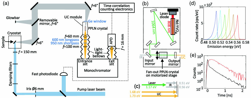
    Fig. 1. (a) Overview of the detection system. An incoming pulsed laser beam (blue) excites a GeSn sample, and the emitted infrared (IR) light (gray) is directed via flat and parabolic mirrors to an upconverter (UC) module, from which the upconverted light (yellow) goes through a monochromator and eventually reaches an avalanche photodiode (APD). The thermal emission of a SiC glowbar can be detected for calibration purposes. (b) Schematic diagram of the UC module. An intracavity field (green) at 1064 nm is mixed with the incoming IR light in a periodically poled lithium niobate (PPLN) crystal, generating the upconverted light (yellow). (c) Schematic representation of involved photon energy ranges, with the two gray and yellow arrows showing the smallest and largest involved energies of the IR and UC light. (d) Measured emission spectra of the glowbar for six different positions of the PPLN crystal motor stage. (e) Example of a decay curve (red) obtained from the GeSn sample at E=0.51  eV, T=20  K, and Φ=2.1×10¹⁵  photons/cm2. The black curve shows the instrument response function (IRF).
    Time-integrated spectra at (a) T=20 K and (b) room temperature. The color of each curve corresponds to the absorbed photon fluence Φ in units of inverse square centimeters (cm−2), referring to the colorbar. In panel (a), the lowest-fluence data was not acquired for the highest emission energies due to low signal-to-noise ratio. The dotted curve represents the shape of the spectrum measured using continuous-wave pumping. The inset in panel (b) schematically shows the band diagram, consisting of the Γ and L valleys of the conduction band and the heavy-hole (hh) and light-hole (lh) valence bands. The energy separations are given in units of milli-electronvolts (meV) and calculated for x=12.5% and −0.55% biaxial strain at T=20 K.
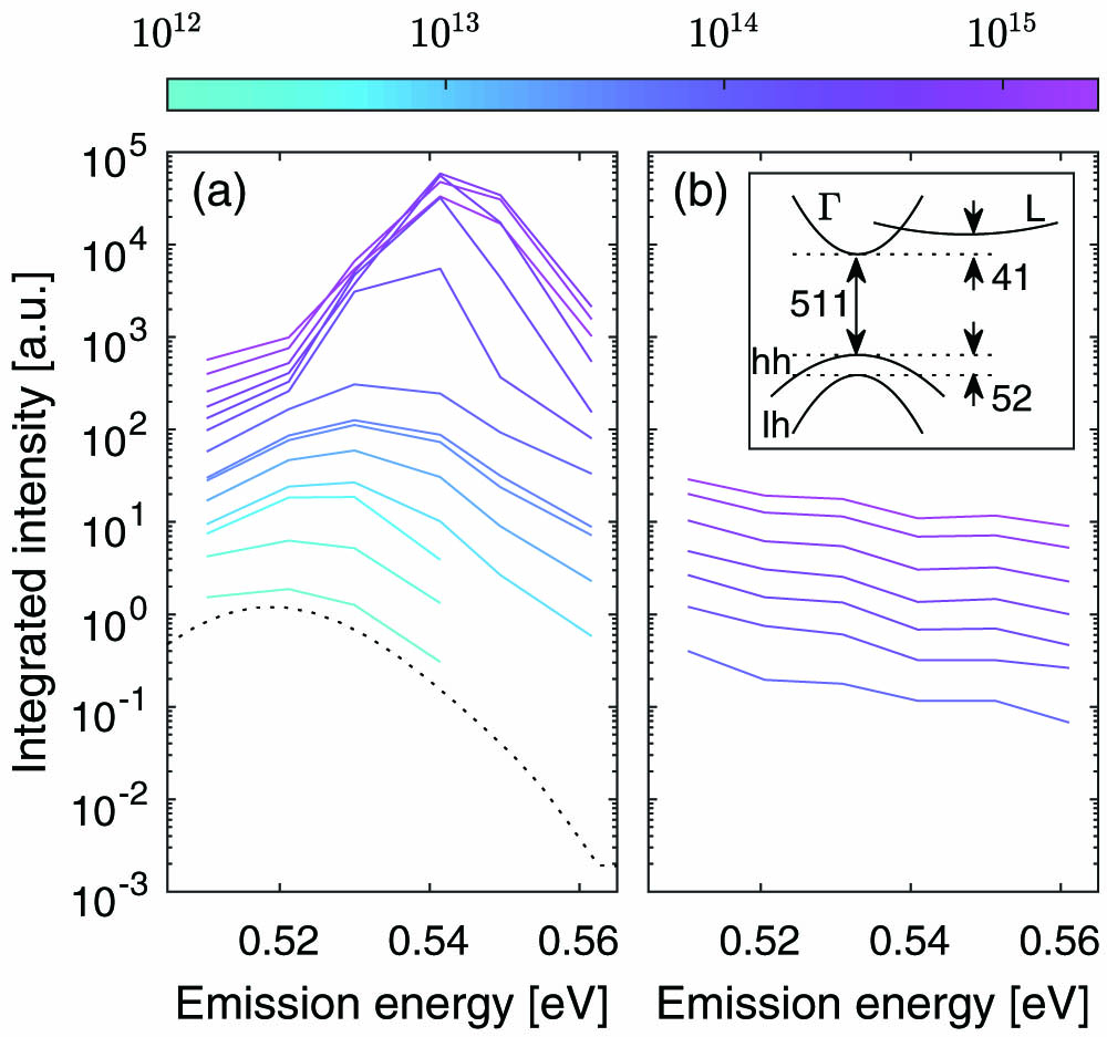
    Fig. 2. Time-integrated spectra at (a) T=20  K and (b) room temperature. The color of each curve corresponds to the absorbed photon fluence Φ in units of inverse square centimeters (cm2), referring to the colorbar. In panel (a), the lowest-fluence data was not acquired for the highest emission energies due to low signal-to-noise ratio. The dotted curve represents the shape of the spectrum measured using continuous-wave pumping. The inset in panel (b) schematically shows the band diagram, consisting of the Γ and L valleys of the conduction band and the heavy-hole (hh) and light-hole (lh) valence bands. The energy separations are given in units of milli-electronvolts (meV) and calculated for x=12.5% and 0.55% biaxial strain at T=20  K.
    (a) Decay curves obtained at T=20 K, E=0.51 eV, and Φ varied according to the color scale (units cm−2). The black curve is (in all panels) the instrument response function. (b) T=20 K and E=0.54 eV with Φ varied according to the color scale. (c) Normalized decay curves at T=20 K and Φ=3.2×1013 cm−2, with colors corresponding to 0.51 eV (blue) and steps of 0.01 to 0.56 eV (red). The smooth curves through the data [in both panels (c) and (d)] represent curve fits. (d) Normalized decay curves obtained at room temperature with Φ=6.9×1014 cm−2.
    Fig. 3. (a) Decay curves obtained at T=20  K, E=0.51  eV, and Φ varied according to the color scale (units cm2). The black curve is (in all panels) the instrument response function. (b) T=20  K and E=0.54  eV with Φ varied according to the color scale. (c) Normalized decay curves at T=20  K and Φ=3.2×10¹³  cm2, with colors corresponding to 0.51 eV (blue) and steps of 0.01 to 0.56 eV (red). The smooth curves through the data [in both panels (c) and (d)] represent curve fits. (d) Normalized decay curves obtained at room temperature with Φ=6.9×10¹⁴  cm2.
    In both panels T=20 K, and the shown spectra have been reconstructed as the model fit f evaluated at the times stated on the time axis. (a) Φ=2.0×1015 cm−2 and (b) Φ=3.2×1013 cm−2.
    Fig. 4. In both panels T=20  K, and the shown spectra have been reconstructed as the model fit f evaluated at the times stated on the time axis. (a) Φ=2.0×10¹⁵  cm2 and (b) Φ=3.2×10¹³  cm2.
    In all panels, the curves are colored according to E from 0.51 eV (blue) to 0.56 eV (red) in steps of 0.01 eV. (a) Mean decay times at T=20 K. The black data points represent the intensity-weighted mean decay time. (b) Mean decay times at room temperature (RT). (c) Time-integrated intensity at T=20 K. The black data points are the sum of all colored data points. Dashed line: double-logarithmic slope=0.98. (d) Time-integrated intensity at RT. Dashed line: slope=1.6.
    Fig. 5. In all panels, the curves are colored according to E from 0.51 eV (blue) to 0.56 eV (red) in steps of 0.01 eV. (a) Mean decay times at T=20  K. The black data points represent the intensity-weighted mean decay time. (b) Mean decay times at room temperature (RT). (c) Time-integrated intensity at T=20  K. The black data points are the sum of all colored data points. Dashed line: double-logarithmic slope=0.98. (d) Time-integrated intensity at RT. Dashed line: slope=1.6.
    (a) Emission spectra of the GeSn sample for different temperatures. The circles show the measured spectra, and the solid curves represent Gaussian functions fitted to a region near the maximum of the spectra. (b) The circles denote the fitted peak position, and the dotted and dashed curves show, respectively, the calculated bandgap energy for a Sn concentration of 12.0% and 12.5% plus 12kT. The biaxial strain is assumed to be −0.55% (compressive). (c) The fitted Gaussian peak area of the emission spectra.
    Fig. 6. (a) Emission spectra of the GeSn sample for different temperatures. The circles show the measured spectra, and the solid curves represent Gaussian functions fitted to a region near the maximum of the spectra. (b) The circles denote the fitted peak position, and the dotted and dashed curves show, respectively, the calculated bandgap energy for a Sn concentration of 12.0% and 12.5% plus 12kT. The biaxial strain is assumed to be 0.55% (compressive). (c) The fitted Gaussian peak area of the emission spectra.
    Common fitting parameters. In all panels, crosses correspond to fitting after the single-exponential Eq. (C1), whereas circles correspond to the delayed Eq. (C2). Colors represent emission energies from 0.51 eV (blue) to 0.56 eV (red) in steps of 0.01 eV. Panels (a) and (b) show the amplitude A1 at T=20 K and room temperature (RT), respectively. Panels (c) and (d) show the decay time t1 at T=20 K and RT, respectively. Panels (e) and (f) show the reduced χR2 at T=20 K and RT, respectively. Panels (g) and (h) show the time tmax of maximum for the fitting model f(t) at T=20 K and RT, respectively.
    Fig. 7. Common fitting parameters. In all panels, crosses correspond to fitting after the single-exponential Eq. (C1), whereas circles correspond to the delayed Eq. (C2). Colors represent emission energies from 0.51 eV (blue) to 0.56 eV (red) in steps of 0.01 eV. Panels (a) and (b) show the amplitude A1 at T=20  K and room temperature (RT), respectively. Panels (c) and (d) show the decay time t1 at T=20  K and RT, respectively. Panels (e) and (f) show the reduced χR2 at T=20  K and RT, respectively. Panels (g) and (h) show the time tmax of maximum for the fitting model f(t) at T=20  K and RT, respectively.
    Phenomenological FD fitting parameters. Symbols and color coding are identical to those in Fig. 7. Panels (a) and (b) show the FD delay time tFD at T=20 K and room temperature, respectively. Panels (c) and (d) show the FD time width tFD at T=20 K and room temperature, respectively.
    Fig. 8. Phenomenological FD fitting parameters. Symbols and color coding are identical to those in Fig. 7. Panels (a) and (b) show the FD delay time tFD at T=20  K and room temperature, respectively. Panels (c) and (d) show the FD time width tFD at T=20  K and room temperature, respectively.
    (a) Heat capacity of Ge. Blue circles are adopted from Table 8 in Ref. [36] and red squares are adopted from Table I in Ref. [37]. The black curve corresponds to the Debye model of Eq. (D2). (b) Thermal conductivity of Ge. Blue circles are adopted from Table I in Ref. [38] and are valid for a high-purity crystal. Red circles are read off from Fig. 1 of Ref. [39] for sample “Ge11” with a carrier concentration of 2×1018 cm−3. The black curve is a compromise between the red data points and the high-temperature limit of the blue data points following Eq. (D3). (c) Thermal diffusion coefficient, based on the black curves from panels (a) and (b).
    Fig. 9. (a) Heat capacity of Ge. Blue circles are adopted from Table 8 in Ref. [36] and red squares are adopted from Table I in Ref. [37]. The black curve corresponds to the Debye model of Eq. (D2). (b) Thermal conductivity of Ge. Blue circles are adopted from Table I in Ref. [38] and are valid for a high-purity crystal. Red circles are read off from Fig. 1 of Ref. [39] for sample “Ge11” with a carrier concentration of 2×10¹⁸  cm3. The black curve is a compromise between the red data points and the high-temperature limit of the blue data points following Eq. (D3). (c) Thermal diffusion coefficient, based on the black curves from panels (a) and (b).
    All panels show solutions to Eq. (D1) at different times according to the colors specified in panel (c). The vertical dashed lines correspond to the interface between the Ge-VS and the GeSn top layer, and an absorption coefficient of α=(200 nm)−1 was used. Absorbed photon fluences are (a) Φ=2×1015 cm−2, (b) Φ=1014 cm−2, and (c) Φ=1013 cm−2.
    Fig. 10. All panels show solutions to Eq. (D1) at different times according to the colors specified in panel (c). The vertical dashed lines correspond to the interface between the Ge-VS and the GeSn top layer, and an absorption coefficient of α=(200  nm)1 was used. Absorbed photon fluences are (a) Φ=2×10¹⁵  cm2, (b) Φ=1014  cm2, and (c) Φ=1013  cm2.
    Brian Julsgaard, Nils von den Driesch, Peter Tidemand-Lichtenberg, Christian Pedersen, Zoran Ikonic, Dan Buca. Carrier lifetime of GeSn measured by spectrally resolved picosecond photoluminescence spectroscopy[J]. Photonics Research, 2020, 8(6): 788
    Download Citation