Brian Julsgaard, Nils von den Driesch, Peter Tidemand-Lichtenberg, Christian Pedersen, Zoran Ikonic, Dan Buca, "Carrier lifetime of GeSn measured by spectrally resolved picosecond photoluminescence spectroscopy," Photonics Res. 8, 788 (2020)
Copy Citation Text
We present an experimental setup capable of time-resolved photoluminescence spectroscopy for photon energies in the range of 0.51 to 0.56 eV with an instrument time response of 75 ps. The detection system is based on optical parametric three-wave mixing, operates at room temperature, has spectral resolving power, and is shown to be well suited for investigating dynamical processes in germanium-tin alloys. In particular, the carrier lifetime of a direct-bandgap film with concentration and biaxial strain is determined to be at a temperature of 20 K. A room-temperature investigation indicates that the variation in this lifetime with temperature is very modest. The characteristics of the photoluminescence as a function of pump fluence are discussed.
1. INTRODUCTION
Germanium-tin alloys are promising materials for electro-optical devices compliant with the existing silicon processing technology [1,2]. It is by now well understood how the composition and strain of films affect the band structure and optical transitions [3,4], and suitable growth techniques have been developed [5,6] for growing direct-bandgap materials of a sufficient quality to obtain laser action [7–10]. Even though some knowledge exists on structural point [11] and extended [12] defects, their impact on the charge carriers remains unresolved, with researchers often resorting to qualified guessing for the carrier lifetimes [13,14]. Here we measure the carrier lifetime by time-resolved photoluminescence spectroscopy, using nonlinear optical upconversion techniques and a fast commercial silicon-based detector. It is demonstrated that spectral resolving power is important for correct interpretation of the decay dynamics and paves the way toward further investigations of optical, electrical, and thermal properties of GeSn alloys.
2. EXPERIMENTAL METHODS
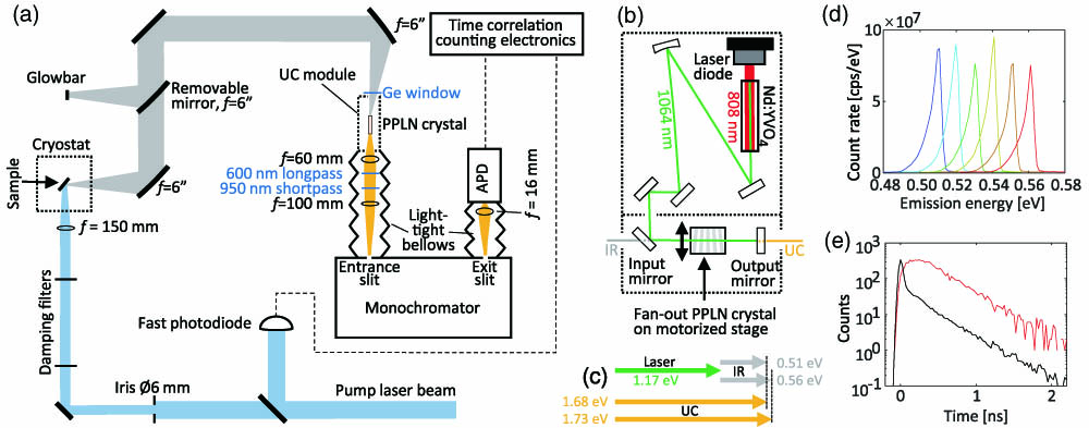
Time-resolved photoluminescence spectroscopy (TRPLS) is an obvious tool for investigating dynamical processes in laser materials. When a short excitation pulse is applied to a semiconductor material, the decaying light curve from radiative recombination of electrons and holes provides direct information on the carrier lifetime. In appropriately designed experiments, such light curves enable the revelation of the underlying dynamical processes like Shockley–Read–Hall (SRH) bulk and surface recombination [15], radiative and Auger recombination [16], as well as carrier diffusion [17]. Applying TRPLS to GeSn materials is a challenge due to the scarce availability of fast detectors in the relevant wavelength range, typically around 2.5 μm. Time-resolved measurements have previously been performed using superconductor nanowire detectors [18,19]; however, they require cryogenic cooling for optimal operation. Our work is based on a technical solution operating at room temperature. The optical experimental setup consists mostly of standard commercial components, i.e., a pumping laser, a grating-based monochromator, an avalanche photodiode (APD), a fast reference photodiode, and an electronic time correlator; see Fig. 1(a). The sensitivity to long-wavelength emission is achieved by a home-built upconverter (UC) module placed in front of the monochromator entrance slit. Such a UC module has previously been used for continuous-wave imaging at mid-infrared wavelengths [20] and for nanosecond spectroscopy [21]. This module is shown schematically in Fig. 1(b), and it relies on parametric three-wave mixing, where infrared photons of wavelength , emitted from the sample under investigation, are mixed inside a periodically poled lithium niobate (PPLN) nonlinear crystal with photons from an intracavity laser of wavelength in order to generate upconverted photons of wavelength , which can be detected by the silicon-based APD. This wavelength transformation is the key factor that enables nearly background-free single-photon detection without cryogenic cooling. For the upconversion process to be efficient, the involved photons must fulfill the energy conservation condition with the involved photon energies depicted in Fig. 1(c). The quasi-phase-matching condition must also be met, where the vectors are wave vectors of the involved optical fields and is the wave vector of the periodic poling of the mixing crystal. The poling period varies across the crystal in a fan-out structure, enabling a continuous tuning of the phase-matched wavelength [22]. Figure 1(d) shows examples of measured spectra obtained from the light emitted by a SiC glowbar. For each position of the PPLN crystal, i.e., for each specific poling period, the maximum signal is obtained when the IR photons travel collinearly with the intracavity laser field through the mixing crystal. The tail toward lower emission energies arises from IR light traveling under an angle relative to the intracavity laser. Switching to the temporal characteristics of the detection system, the instrument response function (IRF) was obtained by shining laser pulses of wavelength μ and duration onto the copper sample holder and detecting the scattered photons; see Fig. 1(e). The FWHM time width of the IRF is , and for comparison Fig. 1(e) also shows a decay curve obtained from a GeSn sample using laser pumping at 800 nm.
Figure 1.(a) Overview of the detection system. An incoming pulsed laser beam (blue) excites a GeSn sample, and the emitted infrared (IR) light (gray) is directed via flat and parabolic mirrors to an upconverter (UC) module, from which the upconverted light (yellow) goes through a monochromator and eventually reaches an avalanche photodiode (APD). The thermal emission of a SiC glowbar can be detected for calibration purposes. (b) Schematic diagram of the UC module. An intracavity field (green) at 1064 nm is mixed with the incoming IR light in a periodically poled lithium niobate (PPLN) crystal, generating the upconverted light (yellow). (c) Schematic representation of involved photon energy ranges, with the two gray and yellow arrows showing the smallest and largest involved energies of the IR and UC light. (d) Measured emission spectra of the glowbar for six different positions of the PPLN crystal motor stage. (e) Example of a decay curve (red) obtained from the GeSn sample at , , and . The black curve shows the instrument response function (IRF).
The film under investigation in this work was grown by chemical vapor deposition (CVD) on a Ge-buffered [23] Si(100) substrate to a thickness of 350 nm and a nominal Sn concentration of . A piece of the sample was inserted into a closed-cycle helium cryostat, enabling measurements at temperatures down to 20 K. The sample was excited by a pulsed laser with pulse duration , wavelength 800 nm, and 5 kHz repetition rate, and by using neutral density (ND) filters, the absorbed photon fluence could be adjusted over several orders of magnitude. The sensitivity of the detection system could be adjusted accordingly by varying the entrance and exit slit openings of the monochromator while maintaining the temporal instrument response. Hence, decay curves could be obtained in a broad range of excitation conditions. See Appendix A for further details on the detection system and sample growth.
Sign up for Photonics Research TOC. Get the latest issue of Photonics Research delivered right to you!Sign up now
3. RESULTS
Before entering into a detailed discussion about the temporal characteristics of the light emission, we shall investigate the time-integrated intensity at various fluences and various emission energies within the detection range from 0.51 to 0.56 eV. The integrated intensity is simply computed as the area under the decay curve [exemplified by the red curve in Fig. 1(e)] for each and , and the result is shown in Fig. 2(a) for and in Fig. 2(b) for room temperature. For the 20 K case, a peaked feature centered at 0.52 eV is present at low excitation fluences, shifting slightly toward higher energies with increasing excitation fluence. This peak corresponds to what is normally described as band-edge luminescence on the direct transition between the valley of the conduction band and the heavy-hole top of the valence band [4] [see the inset of Fig. 2(b) for a schematic band diagram]. We reach this conclusion by comparing the spectra to that [dotted curve in Fig. 2(a)] obtained by standard steady-state photoluminescence spectroscopic methods [4,24] and to bandgap energies calculated from well-established material parameters [25]; see Appendix B. The slight blue-shift of the peak with increasing fluence is attributed to state filling [4]. In addition to this “normal” peak at 0.52 eV with FWHM , another narrower peak, with FWHM and centered around 0.54 eV, emerges when the absorbed fluence exceeds . The physical origin of this peak is unknown and will be discussed later. Turning to the room-temperature spectra in Fig. 2(b), the detection range only allows for observing the high-energy tail of the emission spectra, since their peak energy has decreased due to bandgap shrinkage; see Fig. 6 in Appendix B. A time-resolved investigation is still possible, though.
Figure 2.Time-integrated spectra at (a) and (b) room temperature. The color of each curve corresponds to the absorbed photon fluence in units of inverse square centimeters (), referring to the colorbar. In panel (a), the lowest-fluence data was not acquired for the highest emission energies due to low signal-to-noise ratio. The dotted curve represents the shape of the spectrum measured using continuous-wave pumping. The inset in panel (b) schematically shows the band diagram, consisting of the and L valleys of the conduction band and the heavy-hole (hh) and light-hole (lh) valence bands. The energy separations are given in units of milli-electronvolts (meV) and calculated for and biaxial strain at .
In order to distinguish between the two peaks located at 0.52 eV and 0.54 eV, all decay curves obtained at at the emission energy are shown together in Fig. 3(a). The absorbed photon fluence is varied between and , and the decay curves reveal a steady growth of the overall luminescence intensity with while the temporal characteristics of the decay vary only slightly. In contrast, decay curves obtained under similar excitation conditions but observed at show a rapid increase in overall intensity when ; see Fig. 3(b). This increase simply reflects the observation already made in Fig. 2(a), where the entire peak, centered at 0.54 eV, suddenly emerges when . Furthermore, a delayed onset of light emission is clearly seen when the fluence increases even further above . We attribute this delay to transient heating of the GeSn film, which will be discussed more at the end of this section. Comparing Figs. 3(a) and 3(b) at low fluences also reveals a change in the shape of the decay curves. At low emission energy [Fig. 3(a)] the curves appear more flat-topped than at [Fig. 3(b)]. This fact is further elaborated in Fig. 3(c), where the decay curves of all six investigated emission energies are shown together and obtained at a fluence well below the onset of the 0.54 eV peak. Clearly, the high-energy component (red) decays fastest, and the low-energy components show an in-growth as well. To explain our interpretation of this observation, note first that the width of the “normal” peak at 0.52 eV in Fig. 2 is much broader than at . This is attributed to alloy broadening [26], i.e., random variations in the Sn concentration, and systematic variations in the Sn concentration might also play a role. As a consequence, there will be spatial variations in the bandgap energy across the film. The differently colored decay curves in Fig. 3(c) thus mostly represent the light emission from electron-hole pairs at different locations, and the actual shape of individual decay curves will be affected by carrier diffusion. For instance, if an electron-hole pair recombines radiatively at a site with a low bandgap energy [contributing to, e.g., the blue decay curve in Fig. 3(c)], there can be a subsequent diffusion of charge carriers from neighboring sites of higher bandgap energy, which will extend the duration of the blue curve. In contrast, the sites with a large bandgap energy will be depleted faster, since an in-diffusion of neighboring charges would now be energetically uphill, which is less likely the lower the temperature. This causes the shorter decay time for, e.g., the red decay curve in Fig. 3(c). For increasing temperature, this effect should expectedly become smaller, which is consistent with Fig. 3(d), where the distinction between curve shapes is much smaller. The actual in-growth of the low-energy curves in Fig. 3(c) can be explained as follows. When electrons and holes are generated by the optical excitation pulse, they are expected to thermalize with the lattice within a picosecond [27] and thus immediately start to emit light according to the spatial distribution of charge carriers as discussed above. However, the penetration depth of the excitation pulse at 800 nm wavelength is likely to be similar to the Ge value of [28], but possibly smaller due to the Sn content and nonlinear absorption. This means that the charges generated initially near the sample surface must diffuse a long distance in order to populate all low-energy sites deeper inside the 350 nm thick film, which causes the delayed onset.
Figure 3.(a) Decay curves obtained at , , and varied according to the color scale (units ). The black curve is (in all panels) the instrument response function. (b) and with varied according to the color scale. (c) Normalized decay curves at and , with colors corresponding to 0.51 eV (blue) and steps of 0.01 to 0.56 eV (red). The smooth curves through the data [in both panels (c) and (d)] represent curve fits. (d) Normalized decay curves obtained at room temperature with .
In order to complement the above qualitative discussion of the decay curves with a more quantitative analysis, curve fitting is performed for all decay curves. A mathematical decay model can be convolved [29] with the measured instrument response function to yield the curve fit model . Examples of such fits are provided with smooth curves in Figs. 3(c) and 3(d). In a few cases, it is sufficient to use a single-exponential decay model , where is an amplitude and the decay time. In the remain cases, the curves have been fitted to the function . Although the denominator is inspired by the Fermi–Dirac (FD) distribution function, and although we denote the extra two parameters as the FD delay and the FD width , it should be pointed out that this decay model is purely phenomenological. Hence, the involved parameters should be interpreted with care. Still, the model is remarkably successful in fitting essentially all decay curves. The fitting parameters are described further in Appendix C.
With the fitted decay models at hand, it is now possible to reconstruct the time evolution of the emission spectra by simply displaying versus emission energy at different times. This is done in Fig. 4 for both a high and low fluence, i.e., both well above and below the onset at for the spectral peak centered at 0.54 eV. Figure 4(a) confirms that this entire peak reaches its maximum emission only after (at the highest fluence). Likewise, Fig. 4(b) confirms a slight red-shift over time for the low-fluence case. For further clarity, an animation of the time evolution of the spectra is given in Visualization 1.
Figure 4.In both panels , and the shown spectra have been reconstructed as the model fit evaluated at the times stated on the time axis. (a) and (b) .
The average decay time has been calculated for each decay curve and plotted in Fig. 5(a) at . The distinction between the different emission energies, already seen qualitatively in Fig. 3(c), is clearly emerging from this figure: the emission at low energy (blue data points) generally lasts longer than in the case at high energy (red data points), which at low fluences (below the 0.54 eV peak onset) confirms the state-filling effect of the degenerate charge carriers. To relate these mean decay times of individual light curves to the actual carrier lifetime of the optically generated electrons and holes, consider Fig. 5(c), where the colored data points correspond to exactly the same time-integrated intensity as can be found in Fig. 2(a), but they are now displayed as a function of fluence for each emission energy. Since the investigated emission energies are essentially evenly spaced and cover almost the entire spectrum, it is reasonable to consider the sum of intensities over emission energy (black data points) as a measure of the total amount of light emitted from the material. In addition, since this total amount of light scales proportionally to the absorbed photon fluence (just below the 0.54 eV peak onset as documented by the black dashed line) and therefore proportionally to the generated concentration of charge carriers, the mean decay time of this total intensity must reflect exactly the mean decay time of charge carriers. Mathematically, this means that the carrier decay time is nothing but the average of the individual mean decay times [colored data points in Fig. 5(a)] weighted by the integrated intensity, resulting in the black data points in Fig. 5(a). These data points are very similar in the linear regime and lead to our conclusion about the carrier lifetime , where the uncertainty includes an estimate of systematic errors. We note that the convolution of decay models with the well-determined IRF enables uncertainties below the instrument response time of . A similar analysis could be attempted for the room-temperature data [shown in Figs. 5(b) and 5(d)]. However, since the detection range only covers the high-energy tail of the emission spectrum, and since a linear regime of total intensity with fluence is not found, we must resort to a qualitative discussion of the decay times displayed in Fig. 5(b). The distribution of decay times around is quite narrow due to the more nondegenerate electron and hole distributions. Since the measurements probe the high-energy tail of the emission spectrum, the shown decay times expectedly slightly underestimate the luminescence decay time of the entire spectrum. Furthermore, since the luminescence signal grows faster than linearly with the absorbed photon fluence, the carrier lifetime is most likely even longer. Despite these qualitative observations at room temperature, the variation of carrier lifetime from to room temperature is definitely very modest. This leads to the conclusion that variations in the SRH recombination rate play a minor role in the rather drastic reduction in emission yield with increasing temperature (see Fig. 6 in Appendix B), i.e., there must be a physical mechanism that lowers the emission efficiency but does not lead to an increased loss rate of electron-hole pairs. Previously, the decreasing emission yield with increasing temperature of Fig. 6 has been attributed to a combination of an increased SRH recombination rate and population of the L valley in the conduction band [4,7]. We also note that the low-temperature carrier lifetimes [black data points below in Fig. 5(a)] as well as the measured room-temperature mean decay times in Fig. 5(b) are independent of , and in turn independent of carrier concentration. This shows that Auger recombination does not make a major contribution to the stated lifetimes.
Figure 5.In all panels, the curves are colored according to from 0.51 eV (blue) to 0.56 eV (red) in steps of 0.01 eV. (a) Mean decay times at . The black data points represent the intensity-weighted mean decay time. (b) Mean decay times at room temperature (RT). (c) Time-integrated intensity at . The black data points are the sum of all colored data points. Dashed line: double-logarithmic . (d) Time-integrated intensity at RT. Dashed line: .
Figure 6.(a) Emission spectra of the GeSn sample for different temperatures. The circles show the measured spectra, and the solid curves represent Gaussian functions fitted to a region near the maximum of the spectra. (b) The circles denote the fitted peak position, and the dotted and dashed curves show, respectively, the calculated bandgap energy for a Sn concentration of 12.0% and 12.5% plus . The biaxial strain is assumed to be (compressive). (c) The fitted Gaussian peak area of the emission spectra.
Returning to the increasingly delayed onset of emission with increasing for the highest fluences in Fig. 3(b), the above discussion of emission efficiency versus temperature can be speculated to also being relevant for the 0.54 eV peak. The excess energy of photons from the excitation laser pulse can cause a temperature increase of the material, thereby temporarily lowering the emission efficiency. In Appendix D it is shown that both the fluence threshold and the characteristic time delay required for the film to cool down and restore its efficient light emission are consistent with a simple heat-transport model, based on known thermal properties of germanium.
4. DISCUSSION
It should be underlined that the spectral resolving power of the optical detection system is important in order to get the correct interpretation of the data. If, for instance, some random emission energy was chosen to represent the entire population of carriers, any decay time between 100 and 300 ps could have been found according to Fig. 5(a). Similarly, the indications of state filling and carrier diffusion from the differently shaped decay curves in Fig. 3(c) do also rely on this spectral resolving power. Furthermore, a large dynamic range and a careful determination of the IRF are also needed for accurate determination of the temporal dynamics at the time scales studied here. We note that a previous investigation [19] has measured the carrier lifetime of an indirect-bandgap film to be a few nanoseconds using a superconductor nanowire detector. Despite the fact that no details were published about the emission energies, making the interpretation a bit harder, the one-order-of-magnitude difference in decay time relative to our findings seems trustworthy. We attribute the longer decay time in the previous study to the significantly smaller Sn concentration. The higher Sn concentration of our sample is expected to cause a higher amount of material defects and in turn a faster SRH recombination rate. We also note that no efforts were undertaken to passivate the surface of our sample. In another recent study of films crystallized on insulators from amorphous GeSn [30], a gain lifetime of 70–100 ps was determined at various high-level injection concentrations and at for a sample with using optical pump-probe techniques to measure the temporal evolution of the optical transmission. Since the crystallized GeSn could possibly contain a higher concentration of defects than epitaxially grown GeSn (despite the lower Sn concentration), the above lifetime range seems consistent with our observed room-temperature decay times from Fig. 5(b).
Returning to the spectral peak centered at 0.54 eV emerging at high fluences, we can only speculate about the origin. Dividing its onset fluence of by the film thickness of 350 nm leads to a rather high characteristic excess carrier concentration of , and it cannot be excluded that amplified spontaneous emission [31] is somehow involved. However, the GeSn material contains many defects, and alternative possibilities exist, e.g., that the 0.52 eV peak originates from excitons bound to defects, and the 0.54 eV peak originates from free excitons emerging when the carrier concentration exceeds the defect concentration [32]. In this respect, it should be noted that an unintentional p-type doping concentration of has been estimated by electrochemical capacitance-voltage profiling. Further investigations are required to clarify this point.
5. CONCLUSION
We have demonstrated an optical detection system capable of fast time resolution, spectral selectivity, and large dynamic range. This enabled the very precise determination of the carrier lifetime of our particular GeSn sample and opened the possibility to acquire time-resolved emission spectra. The temporal evolution of a collection of decay curves, obtained at various emission energies and excitation fluences, gave strong indications of both carrier diffusion and heat transport. Hence, the optical detection system paves the way toward interesting future investigations of dynamical processes in GeSn semiconductors and possibly toward determination of important material parameters relevant for GeSn laser technology.
Acknowledgment
Acknowledgment. B. Julsgaard is grateful to Henrik B. Pedersen for assistance with timing electronics in the early stages of this work.
APPENDIX A: DETECTION SYSTEM AND SAMPLE GROWTH
The laser excitation pulses of wavelength 800 nm were generated by a Spectra-Physics Solstice Ace femtosecond laser with deliberate nonperfect pulse compression to obtain ~ pulse duration. The absorbed photon fluence was calculated from the measured laser beam power, calibrated transmissivities of ND filters, the laser spot diameter (1.6 mm) at the sample, the angle of incidence (52°), and the measured reflectivity (25%) of the sample. An optical parametric amplifier (TOPAS) was used to generate the laser pulses of wavelength ~μ for the IRF calibration.
The home-built UC module was operated with a power of ~ for the intracavity laser field of wavelength 1064 nm and beam radius 180 μm, the latter figure defining the active detection area. The fan-out PPLN crystal was purchased from HC Photonics with a varying poling period from 17 to 19 μm. The inherent FWHM resolution of the UC module, as represented by the spectra in Fig. 1(d), was ~. The quantum efficiency of the collinear upconversion was estimated to be ~; see Ref. [20]. The monochromatic acceptance angle is small (estimated ) due to the crystal length of ~, i.e., the phase-matched wavelength increases for noncollinear interaction [21], as seen by the tail on the low-energy side of the spectra in Fig. 1(d). Further information about the design of the UC module can be found in Ref. [20].
The monochromator was a McPherson model 218 equipped with a 1200 g/mm grating and a single-photon-counting APD (model MPD-100-CTB from PicoQuant) for light detection. The monochromator further narrowed the spectral resolution, depending on the chosen slit sizes, to the range 0.2–4 meV. This also reduced the dark count rate arising from a broad spectrum of photons from the UC module. The measured instrument response function [black curve in Fig. 1(e)], including the exponential tail, matched very well the specifications from the manufacturer. The fast reference photodiode assembly (TDA 200) and time-correlating electronics board (TimeHarp 260) were also purchased from PicoQuant.
For calibration of spectral response, a SiC glowbar (model IR-Si207) from Scitec Instruments was operated at 1200°C. SiC is known to have a high emissivity [33] and hence well approximates a black-body emitter. The operating temperature was chosen such that the emission spectrum became essentially flat within the photon-energy detection range 0.51–0.56 eV.
The GeSn sample was grown in an industry-compatible CVD reactor using digermane and tin tetrachloride precursors. Removal of the native oxide and pre-epi cleaning were performed using hydrofluoric acid vapor chemistry and an in situ hydrogen bake. Composition and strain of the resulting films were determined using Rutherford backscattering spectrometry and X-ray diffraction reciprocal space mapping.
APPENDIX B: CONTINUOUS-WAVE CHARACTERIZATION
In addition to the time-resolved emission spectra discussed in the main text, this section describes a set of steady-state emission spectra obtained by pumping the sample with a chopped frequency-doubled continuous-wave diode laser (wavelength 532 nm) with a power of 100 mW. The luminescence was collected using a Fourier transform infrared (FTIR) spectrometer in a step-scan mode and detected by a liquid-nitrogen-cooled InSb detector. The impact of thermal radiation was further eliminated by an optical filter with cutoff wavelength of 3 μm. The resulting spectra are shown in Fig. 6(a) for various sample temperatures. These spectra are not entirely symmetric; however, the shapes are largely Gaussian, and the spectral peaks have been fitted to a function , where is an amplitude factor, is the full-width at half maximum, and is the background. The peak positions are shown in Fig. 6(b), and they are compared to calculated bandgap energies for the direct transition between the valley in the conduction band and the heavy-hole valence band maximum plus a contribution accounting for the fact that optical recombination of carriers takes place at a distribution of energies above the band-edge threshold. The observed peak positions correspond well to expectations for a Sn concentration in the range 12.0%–12.5%, and small deviations across the wafer from the measured concentration of are acceptable within experimental tolerances. The spectrum in Fig. 6(a), with peak position at 0.52 eV, is reproduced as the dotted curve in Fig. 2(a). By comparison, these findings strongly indicate that the luminescence obtained with low pump fluences in Fig. 2(a) has the same physical origin as the steady-state spectra discussed above and normally attributed to band-edge luminescence. The alloy band structure was calculated including the band bowing, strain [34], and finite-temperature effects (Varshni formula [35]) with the parameters from Table 1 in Ref. [25]. Figure 6(c) shows the fitted Gaussian peak areas, and it can be seen that the photoluminescence yield drops by 2 orders of magnitude if the temperature is raised from 20 K to room temperature.
APPENDIX C: CURVE FITTING PARAMETERS
As explained in the main text, the decay curves have been modeled by either a single-exponential decay or by a delayed exponential decay following the mathematical function Figures 7(a)–(d) show the fitted parameters and for and for room temperature. Error bars represent the statistical error in the fitting procedure, which arises from the counting statistics of the photon detection. These results resemble to a large extent the findings of Fig. 5. Noteworthy is the fact that tends to decrease for the very highest fluences and [Fig. 7(c)], while the mean decay time in contrast tends to increase or remain constant in this fluence range according to Fig. 5(a). Hence, the results indicate that the increase in mean decay time, as discussed in the main text, does not correspond to a slower decay rate but rather an increasing delay before the onset of light emission. This is consistent with the result of Fig. 7(g), which shows the time where the fitting function attains its maximum. Figures 7(e) and 7(f) show the reduced , which should be close to unity if the deviation between data points and the fitting model is solely caused by statistical fluctuations of the photon counting process. Obviously, essentially all decay curves have been fitted well. The only exception (with ~) still captures the shape of the experimental decay curve reasonably (not shown).
Figure 7.Common fitting parameters. In all panels, crosses correspond to fitting after the single-exponential Eq. (C1), whereas circles correspond to the delayed Eq. (C2). Colors represent emission energies from 0.51 eV (blue) to 0.56 eV (red) in steps of 0.01 eV. Panels (a) and (b) show the amplitude at and room temperature (RT), respectively. Panels (c) and (d) show the decay time at and RT, respectively. Panels (e) and (f) show the reduced at and RT, respectively. Panels (g) and (h) show the time of maximum for the fitting model at and RT, respectively.
Figure 8.Phenomenological FD fitting parameters. Symbols and color coding are identical to those in Fig. 7. Panels (a) and (b) show the FD delay time at and room temperature, respectively. Panels (c) and (d) show the FD time width at and room temperature, respectively.
APPENDIX D: ESTIMATION OF THE HEAT TRANSPORT DYNAMICS
Consider the internal energy per volume of the GeSn film. If the temperature is raised by , the corresponding change in is , where is the mass density and is the temperature-dependent specific heat capacity. This internal energy is connected to the heat current through the continuity equation , where corresponds to the depth into the sample in a one-dimensional description of the heat flow. The heat current is driven by a gradient in temperature , where is the temperature-dependent thermal conductivity. Putting all this together, and using the chain rule when calculating the derivative with respect to time , one finds where is the temperature-dependent thermal diffusion coefficient. In order to solve this diffusion equation, the involved material parameters and must be known. This is not the case for GeSn, but we shall make a qualified guess based on published values for germanium. Consider first the lattice heat capacity, which exists as tabulated values from 12 K to more than 600 K; see Fig. 9(a). The black curve in this figure has been chosen as a pragmatic and simple compromise following the Debye model: where and were adjusted to match the tabulated data reasonably. The electronic heat capacity is per electron or hole, where is Boltzmann’s constant. For the carrier concentrations and temperatures studied here, the lattice heat capacity is always the dominating contribution.
Figure 9.(a) Heat capacity of Ge. Blue circles are adopted from Table 8 in Ref. [36] and red squares are adopted from Table I in Ref. [37]. The black curve corresponds to the Debye model of Eq. (D2). (b) Thermal conductivity of Ge. Blue circles are adopted from Table I in Ref. [38] and are valid for a high-purity crystal. Red circles are read off from Fig. 1 of Ref. [39] for sample “Ge11” with a carrier concentration of . The black curve is a compromise between the red data points and the high-temperature limit of the blue data points following Eq. (D3). (c) Thermal diffusion coefficient, based on the black curves from panels (a) and (b).
Figure 10.All panels show solutions to Eq. (D1) at different times according to the colors specified in panel (c). The vertical dashed lines correspond to the interface between the Ge-VS and the GeSn top layer, and an absorption coefficient of was used. Absorbed photon fluences are (a) , (b) , and (c) .
We stress that the above considerations are only a rough estimate of the temperature effects. The thermal parameters in Fig. 9 are valid for pure germanium, not GeSn, and the thermal conductivity represents a best guess neglecting dependencies on the electron/hole concentration. The results are thus ballpark estimates. Furthermore, the assumed penetration depth is valid for pure Ge and is likely to be smaller for pulsed excitation of GeSn. Finally, the transient temperature increase would persist for a slightly longer time if we were to also include the heat generation during SRH recombination. Anyway, the above estimates do not contradict the experimental findings, which makes it reasonable to hold on to the hypothesis that transient heating of the GeSn film causes the pronounced delay in emission shown in Figs. 3(b) and 4.
[36] U. Piesbergen. Die durchschnittlichen atomwärmen der AIIIBV-halbieiter AlSb, GaAs, GaSb, InP, InAs, InSb und die atomwärme des elements germanium zwischen 12 und 273°K. Z. Naturforschg., 18A, 141-147(1963).
[39] J. A. Carruthers, T. H. Geballe, H. M. Rosenberg, J. M. Ziman. The thermal conductivity of germanium and silicon between 2 and 300°K. Proc. R. Soc. Lon. Ser. A, 238, 502-514(1957).
Brian Julsgaard, Nils von den Driesch, Peter Tidemand-Lichtenberg, Christian Pedersen, Zoran Ikonic, Dan Buca, "Carrier lifetime of GeSn measured by spectrally resolved picosecond photoluminescence spectroscopy," Photonics Res. 8, 788 (2020)