Chang-Yi PAN, Hao MOU, Xiao-Mei YAO, Tao HU, Yu WANG, Chao WANG, Hui-Yong DENG, Ning DAI. High performance Ge:B blocked impurity band detector developed using near-surface processing techniques[J]. Journal of Infrared and Millimeter Waves, 2022, 41(2): 389
Copy Citation Text
Blocked impurity band (BIB) detectors are the state-of-the-art choice for far infrared astronomical observation. Ge:B BIB far infrared detector has been successfully developed using near-surface processing techniques. The spectral response covers a wide range from 50 cm-1 to 400 cm-1. At a temperature of 3.5 K and a working voltage of 30 mV, the detector exhibits a highly competitive responsivity of 21.46 A?W-1 and a highly competitive detectivity of 4.34×1014 cm?Hz1/2?W-1 at the peak response of 84.9 cm-1. The influence of the interfacial barriers on the spectral response is investigated. A new excitation model that the carriers in the contact regions can be excited over the interfacial barriers is proposed. Moreover, a new method to enhance the relative response intensity of BIB detectors in the low wavenumber region is found.
Far infrared electromagnetic spectrum plays an important role in astronomical observation since the emission from lots of low temperature objects in the universe lies in this spectrum range. There are various far infrared detectors,such as transition edge sensor(TED)detector,kinetic inductance(KID)detector,hot electron bolometer(HEB)detector,superconducting tunnel junction(STJ)detector and blocked impurity band(BIB)detector[1-6]. Among them,BIB detector has the advantages of high detectivity,high response speed and good anti-radiation performance,making it the state-of-the-art choice for astronomical observation in far infrared band and widely used in various astronomical telescopes.
BIB detector was first conceived and demonstrated by Petroff and Stapelbroek at Rockwell International Science center in 1980[7-8]. It is a derivation of the regular extrinsic photoconductors and its cutoff wavenumber in the low wavenumber region is mainly determined by the activation energy of the impurity. Generally,Si-based,Ge-based and GaAs-based BIB detector can respond up to 250 cm-1,50 cm-1 and 33.3 cm-1,respectively[9-13]. The typical BIB detector consists of four functional regions:one medium doped absorbing region(AR),one high purity blocking region(BR)and two degenerated doped contact regions(CRs)[14-15]. The impurity concentration in the absorbing region is a little high so that considerable orbital overlap between the individual impurity levels causes them merge into an impurity band. The formation of the impurity band can extend the spectral response,but the hopping conduction in the impurity band may contribute to a considerable dark current[16-17]. In contrast,in the blocking region,the impurity concentration is very low and there is no impurity band. Therefore,the dark current associated with hopping conduction are blocked. For efficient functioning of BIB detector,the doping concentrations in the different functional regions need to be accurately controlled which increases the difficulty of device preparation. Initially,Si-based BIB detectors were mainly developed by epitaxial techniques which can obtain a deeply doped absorbing region easily. However,it encountered a lot of difficulties to develop Ge-based and GaAs-based BIB detectors by epitaxial methods[18-19]. Moreover,the epitaxial process is usually troublesome and expensive. To circumvent the disadvantages of epitaxial methods,Jeffery W. Beeman proposed a novel method to fabricate BIB detectors using near-surface processing techniques[20]. With this new method,the absorbing region and the contact regions are formed by ion implantation and the high purity substrate serves as the blocking region. Since the new method was proposed,it has been extensively researched[10,21].
Due to the bandgap narrowing effect,the valence band maximum(or the conduction band minimum)differs in the different functional regions for p-type(or n-type)BIB detector[22-24]. This causes energy band barriers at the interface between the different functional regions. Recently,some researchers have demonstrated the existence of the interfacial barrier between AR and BR and have studied the influence of the interfacial barrier on the spectral response[25-26]. However,the barriers between CRs and their adjacent regions have always been ignored. There is no doubt that these barriers will have a great impact on the performance of BIB detectors and are urgently to be studied.
In this work,a planar Ge:B BIB detector was developed using near-surface processing techniques. The preliminary results of the dark current,blackbody response and spectral response reveals a highly competitive performance of our detector in the far infrared band. We have investigated the influence of the interfacial barriers on the spectral response. On one hand,the holes in CRs can be photoexcited to cross the interfacial barriers,extending the spectral response in the high wavenumber region. On the other hand,the increase of voltage can increase the probability of carriers tunneling through the interfacial barrier,enhancing the spectral response in the low wavenumber region.
1 Experiments
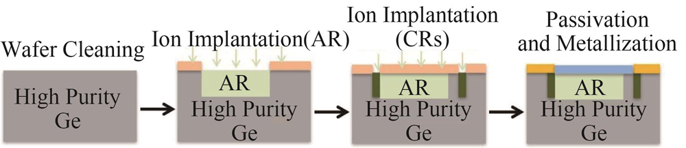
The samples were fabricated using near-surface processing techniques,as illustrated by Fig. 1. The starting material was a high purity Ge substrate with room temperature resistivity greater than 35 . In order to obtain a large doping depth,we choose boron(B)with a small atomic mass as the dopant. Moreover,the smaller the mass of the implanted impurity,the smaller the damage to the crystal lattice. Photolithography was used to form the patterns of AR and CRs on the substrate surface and the 3 thick photoresist was used as the mask for subsequent ion implantation. The implantation process was carried out by five steps with different energies and doses. Figure 2 shows the doping profiles simulated by Technology Computer Aided Design(TCAD),and measured by secondary ion mass spectroscopy(SIMS)in AR. The resultant implantation depth was about 1.1 . In AR,the target concentration was 5×1016 cm-3 while the measured concentration was about 4×1016 cm-3. We think this may be the result of the channel effect. In CRs,the target concentration was 3×1018 cm-3,much lower than that in the previous work. We found that the doping concentration in CRs could affect the interfacial barrier height,thereby affecting the electric field distribution inside the BIB detector. The undoped region between AR and CRs serves as BR. The areas of AR and BR were 1 000m×50m and 1 000 m×10 m,respectively. After implantation,200 nm Si3N4 was deposited by plasma-enhanced chemical vapor deposition(PECVD)technique to protect the surface of the detector and to serve as the anti-reflection layer. We used reactive ion etching(RIE)technique to remove the Si3N4 layer on the surface of CRs. Afterwards,the contact electrode with 20 nm Pd and 200 nm Au was deposited using thermal epitaxial technique and alloyed at 450 for 300 seconds. The resultant Ge:B BIB detector is shown in Fig. 3.
In order to freeze out the carriers in the impurity band,BIB detectors have to work at ultra-low temperature. In the dark current test,we used a closed-loop liquid helium-cooled cryostat(OptistatAC-V),which can provide a temperature range of 2.3∼300 K. In the photocurrent test,we used a vacuum loading continuous flow helium cryostat(Optistat CF-V),which was equipped with a far infrared optical window. IR-301 blackbody system was used in the blackbody response test and Bruker VERTEX 80 V Fourier transform infrared(FTIR)spectrometer was used in the spectral response test.
2 Results and discussions
Operating temperature has a great influence on the dark current of BIB detectors. Figure 4 shows the dark current of Ge:B BIB detector at different temperature. At low temperature(lower than 4 K),there is obviously a breakdown characteristic. Before breakdown,the dark current maintains at the magnitude of 10-10 A. After breakdown,the dark current increases abruptly and approaches saturation quickly. On conventional operation mode(where positive voltage is applied to AR),the breakdown voltages at 2.3 K,3 K,3.5 K and 4 K equal to 220 mV,145 mV,90 mV and 40 mV,respectively. On alternate operation mode(where negative voltage is applied to AR),the breakdown voltages at 2.3 K,3 K,3.5 K and 4 K equal to 140 mV,75 mV,40 mV and 25 mV,respectively. We think the breakdown characteristic is dominated by field-assisted thermal ionization process(Poole-Frenkel effect)[27-28]. At sufficiently low temperature,the holes in the impurity band cannot be thermally excited to the valence band directly. Before the ionization process occurs,there are almost no carriers that can migrate freely and the dark current is very small. However,with the help of the electric field,the holes in the impurity band will be ionized to the valence band. Obviously,as temperature decreases,fewer phonons can participate in the thermal ionization process,thereby the breakdown voltage increases. The dark current exhibits a strong asymmetry versus bias due to the presence of BR[29]. However,at relative high temperature(higher than 4 K),the breakdown characteristic vanishes. Once an external voltage is applied,the dark current increases rapidly. This is because the holes in the impurity band can be thermally excited to the valence band directly and there are many carriers in AR.
Figure 4.Dark current of Ge:B BIB detector at different temperatures
The responsivity of a detector refers to the ration of the output electrical signal to the incident radiation energy. For blackbody response test,the responsivity can be expressed as[30]:
,
where is the photocurrent in response to the blackbody. is the blackbody radiation power and can be calculated by:
,
where is the Stefan’s constant, is the blackbody temperature, is the background temperature, is the blackbody aperture area, is the detector area and is the distance from the detector to the blackbody,respectively. is the far infrared window transmission coefficient and can be calculated by:
,
where is the transmittance function of the far infrared window. is the spectral radiance of the blackbody and can be expressed as:
,
where h is the Planck constant,k is the Boltzmann constant,c is the light velocity and T is the blackbody temperature. Figure 5 shows the responsivity in response to a 1000 K blackbody at 3.5 K. Benefited from the optimization of the device structure and the fabrication process,our detector exhibits a very good response performance. At 30 mV,the responsivity even reaches 1.47 A∙W-1,which is a very high value for the planar detector.
Figure 5.Responsivity in response to a 1000 K blackbody at 3.5 K
The blackbody responsivity reflects the overall response characteristics in the whole range of the spectral response. According to the definition of the blackbody responsivity:
,
where is the absolute spectral response, is the responsivity at , is the relative spectral response,which is equal to / . From Eq. 5, can be expressed as[31]:
.
Now,based on the relative spectral response measured using a FTIR spectrometer,we can calculate the responsivity at a specific wavelength. The relative spectral response measured at 30 mV and at 3.5 K is shown in Fig. 6,covering a broad range from 50 cm-1 to 400 cm-1. The peak response locates at 84.9 cm-1(118 m,11 meV),determined by the ionization energy of B in Ge. At 30 mV,the calculated responsivity at 84.9 cm-1 is 21.46 A∙W-1. The detectivity can be expressed as[30,32]:
,
where is the responsivity, is the elementary charge and is the dark current. At 30 mV,the calculated blackbody detectivity is 2.97×1013 cm∙Hz1/2∙W-1 and the calculated peak detectivity at 84.9 cm-1 is 4.34×1014 cm∙Hz1/2∙W-1.
From Fig. 6,it can also be seen that there is a broad response peak at about 168 cm-1. We think this is caused by the excitation of the interfacial barriers,as illustrated in Fig. 7. As mentioned above,there are three interfacial barriers in a BIB detector due to the bandgap narrowing effect. For p-type Ge,the upward shift of the valence band can be formulated as follows[33]:
,
where N is the impurity concentration. The calculated shift of the valence band for CRs,AR and BR equal to 24.6 meV,3.2 meV and 0 meV,respectively. Therefore,the barrier at the interface between CRs and AR(B1),the barrier at the interface between AR and BR(B2)and the barrier at the interface between BR and CRs(B3)equal to 21.4 meV,3.2 meV and 24.6 meV,respectively. At low temperature,these barriers will inevitably block the transport of the carriers[34-35]. On conventional operation mode,barrier B1 can block the injection of the holes in CRs into AR. On alternate operation mode,barrier B3 can block the injection of the holes in CRs into BR. However,in the presence of infrared radiation,the holes in CRs will be able to cross the interfacial barriers by photoexcitation,named excitation mode by the interfacial barrier. On conventional operation mode,the response peak excited by the interfacial barrier is determined by barrier B1 and locates at 165 cm-1. On alternate operation mode,the response peak excited by the interfacial barrier is determined by barrier B3 and locates at 190 cm-1. The experimentally measured response peak in Fig. 6 is very close to the theoretical calculated value. The response peak is very weak possibly because the surface of CRs is covered with metal electrodes,which blocks most of the infrared radiation.
Figure 7.Two excitation models in Ge:B BIB detector
Compared with barriers B1 and B3,barrier B2 has a small height. However,on conventional operation mode,barrier B2 can still block the transmission of the carriers close to the valence band edge[25]. For the photon with low wavenumber(long wavelength),its energy is small and the energy of the corresponding photoexcited carrier is also small. These low-energy photoexcited carriers are close to the valence band edge and are more easily blocked by barrier B2. In contrast,for the photon with high wavenumber(short wavelength),its energy is large and the energy of the corresponding photoexcited carrier is also large. These high-energy photoexcited carriers are not close to the valence band edge and are not blocked by barrier B2. Therefore,we predict that by increasing the operation voltage,the probability of the carriers tunneling through barrier B2 will increase and the relative response intensity in the low wavenumber region will be enhanced. Figure 8 shows the normalized relative spectral response measured at different voltage at 3.5 K. As expected,as the voltage increases,the relative response intensity increases significantly in the low wavenumber region. The inset of Fig. 8 shows the ratio of the relative response intensity at 40 mV and 10 mV. At 71.35 cm-1,the relative response intensity almost increases seven times. In the wavenumber range from 65.6 cm-1 to 78.2 cm-1,the relative response intensity has enhanced over 100%.
Figure 8.Normalized spectral response at different voltages at 3.5 K,and the inset is the ratio of the relative response intensity at 40 mV and 10 mV
In summary,we have fabricated a planar Ge:B BIB detector,in which photolithography and ion implantation were used to produce the absorbing region and the contact region. From 50 cm-1 to 400 cm-1,the detector exhibits a competitive detection performance. At 3.5 K and 30 mV,the blackbody responsivity attains 1.47 A∙W-1,the blackbody detectivity attains 2.97×1013 cm∙Hz1/2∙W-1,the peak responsivity attains 21.46 A∙W-1 and the peak detectivity attains 4.34×1014 cm∙Hz1/2∙W-1 at 84.9 cm-1. The effects of the interfacial barriers on the spectral response were investigated. We proposed a new excitation model by the interfacial barriers. Employing this new model,the relative response in the high wavenumber region can be better explained. Moreover,we also provide a new route to increase the response intensity in the low wavenumber region.
[5] Kai-Sheng LIAO, Zhi-Feng LI, Chao WANG et al. Si:P blocked impurity band detectors for far infrared detection. Journal of Infrared and Millimeter Wave, 35, 37-41(2016).
[6] Chao WANG, Ning LI, Ning DAI et al. Ion-Implanted Si:As blocked impurity band detectors for VLWIR detection. Journal of Infrared and Millimeter Waves, 39, 290-294(2020).
[7] M Petroff, M G Stapelbroek. Blocked impurity band detectors(1986).
Chang-Yi PAN, Hao MOU, Xiao-Mei YAO, Tao HU, Yu WANG, Chao WANG, Hui-Yong DENG, Ning DAI. High performance Ge:B blocked impurity band detector developed using near-surface processing techniques[J]. Journal of Infrared and Millimeter Waves, 2022, 41(2): 389