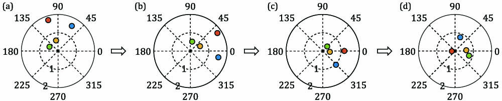
Fig. 1. Graphical explanation of the Min-Max algorithm for a 4×4 processor. Eigenvalues represented by circles in (a)–(d) correspond to colors. (a) Eigenvalues of A shown in the polar coordinate system (all the eigenvalues lie in a half-complex plane, indicating the RICH method converges for a certain ω); (b) rotate all the eigenvalues of A into the right half-plane; (c) eigenvalues of ωoptA; (d) eigenvalues of IN−ωoptA. Now the convergence condition ρ(IN−ωoptA)<1 is satisfied and the fastest convergence rate is also reached.
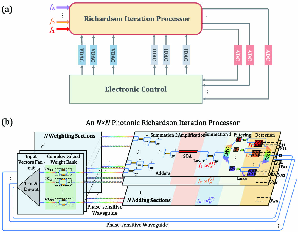
Fig. 2. System architecture of the proposed N×N iterative photonic processor for complex-valued matrix inversion. (a) Workflow of the iterative photonic processing system. The computation includes four main steps: 1) weights loading; 2) gain setting; 3) computation activation; and 4) results readout. VDAC, voltage digital-to-analog converter; IDAC, current digital-to-analog converter. (b) Architecture of an N×N iterative photonic processor. It consists of nine key photonic blocks, including Laser, Summation 1, Input Vectors Fan-Out, Weight Bank, Summation 2, Amplification, Filtering, Detection, and Recirculating Loop. AWG, arrayed waveguide gratings.
Fig. 3. Models of (a) 1-to-N Fan-Out block, (b) Summation block, (c) Weight Bank block, (d) Laser block, (e) Amplification and Filtering blocks, (f) Detection block, and (g) electronic peripherals.
Fig. 4. (a) Typical signal amplitude changes during computation without filtering. (b) Plot of the sine integral function; (c) typical signal amplitude changes during computation after filtering.
Fig. 5. Conceptual figure of an integrated 4×4 inverter (without wavelength multiplexing) where the LDs, BPFs, SOAs, and BPDs are monolithically integrated on-chip. TIAs and digital signal processing (DSP) are used for results readout. One column of the inverse matrix can be computed at a time by turning on one of the LDs, while the complete computation results can be obtained by turning on each of the LDs, respectively, or using multiple copies of the unit shown here.
Fig. 6. (a), (b) Net computing speed of different-sized N×N photonic RIPs on SOI, Si3N4, and IMOS platforms. The light propagation speed is estimated through the effective indices of the waveguides, while the computing speed is estimated considering light propagation speed, loop length, and number of iterations simultaneously. (a) Inversion rate in terms of GInv/s and (b) processing speed in terms of TMAC/s are shown. (c) Power efficiency of different-sized N×N photonic RIPs.
Fig. 7. Matrix weights encoding error for (a)–(e) different DAC bit resolutions and (f) 20 nm wavelength span. Using a 16-bit DAC is enough to guarantee <0.1% relative weight encoding error. The encoding error due to wavelength multiplexing is around 3%. (g) ASE noise powers of different-sized processors when cascading different numbers of SOA stages. Red circles highlight the minimal achievable ASE powers for different-sized processors. Pin,sat at optimal stages of different-sized processors are indicated by the “+” sign. SNR of coherent detection when (h) both thermal noise and shot noise are considered, (i) only thermal noise is considered, and (j) only shot noise is considered. Thermal noise is dominant when signal power is low, while shot noise is dominant when signal power is high.
Fig. 8. (a) Inversion accuracy of different-sized photonic RIPs when input signal powers are different (optical filter BW=64.5 MHz). Values in blue indicate the required iteration numbers for convergence. High-input signal power (>1 dBm) is necessary for ensuring an accuracy of >90% when using wavelength multiplexing technique. (b) Fitted relationship between inversion accuracy and optical filter BW (input signal power is 16.6 dBm) for processor size ranging from 2×2 to 64×64; (c) error breakdown of different-sized photonic RIPs (input signal power is 16.6 dBm).
Method | Constraints on | Key Steps | Complexity |
---|
GE | None | 1) 2) Back substitution | | LUD | None | 1) 2) , 3) Forward substitution: 4) Back substitution: | | CD | Positive definite | 1) 2) , 3) Forward substitution: 4) Back substitution: | | QRD | None | 1) 2) , 3) 4) Back substitution | | SVD | None | 1) 2) | |
|
Table 1. Summary of Main Direct Inversion Methods
Method | Convergence Condition | Iterative Relationship | Complexity | Convergence Rate |
---|
JC | Positive definite | | | Slow | GS | Positive definite | | | Faster than JC | SOR | Positive definite, | | | : accelerate; : GS; : slow down | RICH | Eigenvalues lie in a half-complex plane | | | Depend on the choice of | SD | Positive definite | 1) 2) 3) 4) 5) | | As slow as JC Be accelerated with preconditioning | CG | Positive definite | 1) 2) 3) 4) 5) 6) 7) | | Slightly faster than steepest descent Faster than SOR with preconditioning |
|
Table 2. Summary of Main Iterative Inversion Methods
Photonic Blocks | Components | Functionality |
---|
Laser | CW LDs | Input signal | Summation 1 | Single-stage 50:50 MMI coupler | 1) Couple initial input; 2) add in each iteration | Input Vectors Fan-out | Cascaded 50:50 MMI couplers | Split looped-back signals | Weight Bank | Push-pull MZIs | Encode elements of complex-valued matrix | Summation 2 | Cascaded 50:50 MMI couplers | Add signals up during matrix multiplication | Amplification | Cascaded SOAs | Compensate for on-chip losses | Filtering | AWGs and BPFs | Reduce the ASE noise from SOAs | Detection | Coherent detectors | Inversion results readout | Recirculating Loop | Phase-sensitive waveguides | Provide connections for iterative computation |
|
Table 3. Correspondence between Key Photonic Blocks and Computational Functionalities
Method | Flip-Chip Bonding | Wafer/Die Bonding | | Hetero-epitaxy |
---|
Integration density | Low | Medium | High | High | Efficiency of III-V material use | Medium | Medium | High | Very High | Alignment accuracy | High | High | Hedium | High | Throughput | Medium | High | High | High | Cost | High | Medium | Low | Low | Maturity | Mature | Mature | R&D | R&D |
|
Table 4. Comparison of III-V-on-Si Integration Methods
Component | SOI (μm) | (μm) | IMOS (μm) |
---|
Summation 1 | 20 | 240 | 47 | Input Vectors Fan-out | (2N–1)·72 | (2N–1)·180 | (2N–1)·80 | Weight Bank | 100 | 1100 | 200 | Summation 2 | (2N–1)·90 | (2N–1)·300 | (2N–1)·120 | Amplification | [36] | [37] | [38] | Filtering | 128 | 130 | 200 |
|
Table 5. Length Estimation of an N×N Iterative Photonic Processor on Photonic Integration Platforms
Component | Number | Unit Power (mW) | Total Power (mW) |
---|
Laser | | 69 [45] | 69 N | TOPS | | 0.49 [46] | | SOA | a | 50 [36] | | DAC | | 0.045 [47] | | ADC | | 0.46 [48] | |
|
Table 6. Power Estimation of an N×N Iterative Photonic Processor
Parameter | Value |
---|
Processor size | | Number of random matrix instances | 500/processor size | Half-wave voltage of MZI | 4.36 V [53] | DAC resolution | 16 bits | SOA NF | 3.8 dB [52] | BW of the optical BPF | 64.5 MHz [54] | IL of the optical BPF | 0.2 dB [54] | IL of an MMI coupler | 0.2 dB [29] | IL of a waveguide crossing | 0.019 dB [55] | Center frequency | 193.6 THz | WDM channel spacing | 0.1 nm [28] | Electron charge | | Planck’s constant | | BW of the electronic filter | 32.25 MHz | Boltzmann constant | | Temperature | 300 K | Electronic resistance | 50 Ω |
|
Table 7. Parameters Used in Accuracy Analyses of the Iterative Photonic Processor