
Minjia Chen, Qixiang Cheng, Masafumi Ayata, Mark Holm, Richard Penty. Iterative photonic processor for fast complex-valued matrix inversion[J]. Photonics Research, 2022, 10(11): 2488
- Photonics Research
- Vol. 10, Issue 11, 2488 (2022)
Abstract
1. INTRODUCTION
Complex-valued matrix inversion is a fundamental but computationally expensive linear algebra operation, which is widely used in wireless communication systems [1–5], control systems [6], image processing [7,8], for solving partial differential equations [9], and in many other applications. Complex-valued arithmetic is preferred in many applications due to its better performance compared to real-valued calculations in terms of representational capacity, convergence speed, generalization, and noise robustness [10,11].
Two main advantages of optical matrix computations over traditional digital electronic computations include higher representational efficiency and faster processing speed [12]. First, the real and imaginary parts of one complex-valued number are stored in two registers on traditional electronic computing platforms, with calculations being carried out for real and imaginary parts, respectively. In contrast, an optical signal inherently has two dimensions to encode the real and imaginary parts, which are its amplitude and phase. Second, optical matrix computation allows faster processing speeds through inherent high-speed optical processing. The speeds of digital electronic processors are limited by the transistors’ switching time and time for storing, fetching, and moving intermediate computing results, while the speed of optical matrix computation is solely determined by the signal propagation time in the processor. Photonic integration platforms guarantee ultrafast computing speed due to their ultracompact millimeter-level optical path length. In addition, intermediate computing results can be directly sent to the succeeding components without storing and fetching. In other words, the computation is completed during light propagation.
Optical computing has a long history that dates back to the 1980s [13]. Optical systems for real-valued matrix inversion have been implemented using both free-space optics [14] and fiber-optic networks [15]. Though free-space optical systems have good scalability, the bulky system and high alignment requirements pose big obstacles for practical usage and lead to higher latency than more compact integrated solutions. Fiber-optic systems have large phase fluctuations, making them unsuitable for complex-valued computations. In contrast, photonic integrated platforms provide ultracompact designs and accurate phase control [16–21], which enable the implementation of scalable optical networks for complex-valued matrix inversion.
Sign up for Photonics Research TOC. Get the latest issue of Photonics Research delivered right to you!Sign up now
In this paper, we propose an photonic integrated Richardson iteration processor (RIP) for fast computation of complex-valued matrix inversion and a “Min-Max” algorithm for choosing the optimal parameter for the Richardson (RICH) method for the highest convergence rate, the first time this has been proposed to our knowledge. We also build mathematical models for key building blocks and predict both block-level and system-level performances, which can be used as guidelines for designing an RIP.
The paper is organized as follows. Section 2 reviews the major matrix inversion methods and presents the Min-Max algorithm. Section 3 shows the system architecture of the proposed RIP and the detailed mathematical models of key blocks. Implementations on integrated photonic platforms are also compared. Section 4 presents system-level performance analyses, including speed, power efficiency, accuracy, and scalability based on the models built in Section 3, which can be used as guidelines for choosing input signal powers and bandwidths (BWs) of optical bandpass filters (BPFs) when designing an processor. Section 5 concludes the paper.
2. INVERSION METHODS
Choosing an appropriate computing method is the first concern when we start to build up an optical matrix inverter. In this section, we review two major types of inversion methods, and introduce the Min-Max algorithm for implementing the RICH method in our design.
A. Review of Inversion Methods
In a broad sense, every matrix has its inverse matrix, which is called a generalized inverse or a pseudoinverse [22]. In this paper, we focus on computing the inverses of nonsingular (invertible) square matrices. For a nonsingular matrix ( is a matrix with rows and columns of complex-valued elements), the unique inverse matrix is defined by , where is the identity matrix with ones on the main diagonal and zeros elsewhere.
Calculating the inverse matrix is equivalent to solving linear equations, (), where is the column of the inverse matrix , and is the column of the identity matrix . Furthermore, matrix inversion methods can be classified into direct inversion methods and iterative inversion methods [9].
Direct inversion methods are based on the decomposition of the original matrix . Gaussian elimination (GE), lower-upper decomposition (LUD), Cholesky decomposition (CD), and QR decomposition (QRD) all convert into an upper or lower triangular form, or , and use back or forward substitution to serially compute the inversion results. Singular value decomposition (SVD) decomposes into two unitary matrices , , and one diagonal matrix with nonnegative real elements , taking advantage of the facts that the inverse of a unitary matrix is its conjugate transpose, and the inverse of a diagonal matrix consists of reciprocals of its elements. Table 1 summarizes main direct inversion methods mentioned above for nonsingular matrices [9,23]. The time complexity shown in Table 1 refers to the complexity for solving all equations. Time complexity depicts how the computing time scales with the matrix size, which is usually measured by floating-point operations per second (FLOP/s), since traditionally matrix inversion is computed on digital electronic computers. Though special matrices (such as sparse matrices) require fewer FLOP/s to compute, time complexity without any acceleration is shown here for generality. As shown in Table 1, direct methods all have a time complexity of . Summary of Main Direct Inversion MethodsMethod Constraints on Key Steps Complexity GE None 1) LUD None 1) CD Positive definite 1) QRD None 1) SVD None 1)
Iterative inversion methods compute the inverse matrix by first choosing an approximate initial guess and then updating it in each iteration until it converges. The uniqueness of inverse matrix guarantees the process always converges to the correct solution if the convergence condition is satisfied. Specifically, a solution sequence is generated in order to solve . The iterative relationship is expressed as , which converges to if , where is the ideal solution, and denotes the 2-norm of the matrix. In principle, accurate solutions can be reached after infinite numbers of iterations, while in practice, the iterative process stops after the deviation from the ideal solution is smaller than pre-set values. Iterative inversion methods include classical methods such as Jacobi (JC), Gauss–Seidel (GS), successive overrelaxation (SOR) and RICH, and gradient descent methods such as steepest descent (SD) and conjugate gradient (CG). Table 2 summarizes main iterative methods [9,24–26]. The total computing time depends on both the complexity and the convergence rate. The time complexity shown in Table 2 denotes computing time for each iteration without any acceleration, which is essentially the computing time of a matrix–matrix multiplication. The convergence rate, representing the number of iterations for convergence, depends on the inversion method, the initial guess, , and the required accuracy. Summary of Main Iterative Inversion MethodsMethod Convergence Condition Iterative Relationship Complexity Convergence Rate JC Positive definite Slow GS Positive definite Faster than JC SOR Positive definite, RICH Eigenvalues lie in a half-complex plane Depend on the choice of SD Positive definite 1) As slow as JC Be accelerated with preconditioning CG Positive definite 1) Slightly faster than steepest descent Faster than SOR with preconditioning
In general, direct inversion methods provide more robust solutions in linear systems than iterative inversion methods. Nevertheless, a good initial guess and the use of preconditioning (a means of transforming the original linear equations into one with the same solutions but that is easier to solve) in iterative methods allow for faster computing speed than direct methods, which is especially advantageous for large sparse systems.
B. Richardson’s Method and Min-Max Algorithm
The matrix-form Richardson’s method (the matrix-form RICH method) is shown in Eq. (1),
It is chosen for optical matrix inversion mainly for its easy implementation on integrated photonic platforms. A lack of mature on-chip optical memory [27] restricts the inversion methods to classical iterative methods, since both direct methods and gradient descent methods require storage of intermediate results, while for classical iterative methods, outputs can be easily sent back to inputs through waveguides for iterative computations. Among all the classical iterative methods, the RICH method has the simplest form and the fewest constraints, justifying its usage in computing matrix inverses. To implement the weight matrix in the RICH method optically, we can either use Mach–Zehnder interferometer (MZI) arrays to encode the matrix elements directly or use cascaded MZI meshes to encode the SVD of the weight matrix. Here we choose to use MZI arrays to encode the elements directly to avoid the heavy overhead introduced by SVD.
In the general iterative relationship, , the convergence is guaranteed when the spectral radius satisfies [, is the collection of all the eigenvalues of matrix ]. The convergence rate, , is also determined by the spectral radius. As in the case of the RICH method, the convergence condition is , and the convergence rate is . As long as all the eigenvalues of lie in a half-complex plane, there exists a damping parameter such that the RICH method converges. We propose a Min-Max algorithm to compute the optimal corresponding to the fastest convergence rate. The basic idea is to scale the eigenvalues of matrix up or down into a unit circle centred at (1,0) on the complex plane and minimize the maximal distance of an eigenvalue to the point (1,0). A graphical explanation is shown in Fig. 1.
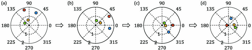
Figure 1.Graphical explanation of the Min-Max algorithm for a
3. PHOTONIC DESIGN
This section consists of three parts. In part A, the system architecture of the proposed RIP is introduced. In part B, the mathematical modeling of key building blocks in the iterative photonic processor is presented. In part C, photonic integration schemes of the iterative photonic processor are discussed and compared.
A. System Architecture
![]()
Figure 2.System architecture of the proposed
B. Modeling
This part introduces the modeling of the iterative system in detail, serving as a preliminary for the system performance analyses in Section 4. Figure 3 shows the models of key building blocks, whose operational principles are characterized by mathematical formulas shown in the following [transverse-electric (TE) mode is assumed in the modeling].
![]()
Figure 3.Models of (a)
1. Input Vectors Fan-Out Block
Figure 3(a) shows the model of a 1-to-NInput Vectors Fan-out block which consists of stages of cascaded 50:50 MMI (multimode interference) couplers. The insertion loss (IL) of each MMI coupler is assumed to be (in dB). and represent the electric fields of the input signal and output signals, respectively. The output electric fields can be expressed by Eq. (2),
The absolute phase shift introduced during propagation is neglected in this model, since it can always be compensated by phase shifters. Only relative phase changes affect the encoded phase information. For a wavelength range of around 20 nm, which is enough to support 200 channels assuming a frequency spacing of 0.1 nm (according to the narrowest spectral grid of the ITU standard for dense wavelength division multiplexing technology [28]), non-ideal coupling ratio and phase deviation are reported over the entire BW [29]. The small deviations can be compensated by adjusting the amplitude and phase of the MZI unit on the corresponding path. Thus, non-ideal coupling is neglected in the model.
2. Summation Block
Figure 3(b) shows the model of the
The MMI combiners can be replaced with MMI couplers with one output port configured as the monitor port for calibrating input phases, as shown in Fig. 2(b). Phase matching is required for both and MMI couplers when configured as adders. For MMI couplers, the phase of the two input signals should be equal, while for MMI couplers, the phase difference between the two inputs should equal 90º. The phase relationship between stage () and of MMI couplers is expressed in Eq. (4),
3. Weight Bank Block
Figure 3(c) shows the model of a single MZI unit of the
The compensation of the non-ideal coupling mentioned in Sections 1 and 2 can be realized by tuning the amplitudes and phases of the MZI weights on corresponding paths.
4. Laser Block
Figure 3(d) shows the model of a continuous-wave (CW) laser source. lasers are used to generate signals with frequencies ranging from to . A higher wall-plug efficiency helps to reduce the power consumption of laser sources. The finite laser linewidth, , is reflected in a randomly fluctuated phase term, , in the generated laser signal, as shown in Eq. (7),
The input signal power, , serves as a normalization power (real-valued unit “1”) for the matrix computation. Laser phase noise normally causes unstable interference when two signals are combined in a summation block. This can be resolved by using a single laser block at each frequency point and splitting the laser signals for homodyne detection as explained in Section 6.
5. Amplification and Filtering Blocks
Figure 3(e) shows the model of the
![]()
Figure 4.(a) Typical signal amplitude changes during computation without filtering. (b) Plot of the sine integral function; (c) typical signal amplitude changes during computation after filtering.
By removing the optical carrier frequency, the spectrum analysis can be shifted to baseband, which simplifies the Fourier analysis.
The baseband spectrum of the signal is shown in Eq. (9),
An optical BW of 2W (Hz) is equivalent to a baseband BW of W (Hz). The filter filters out part of the signal frequency components introduced by the abrupt amplitude changes among different iterations while keeping the DC components intact. The term in Eq. (9) corresponds to a DC term with an amplitude of and a small variation term from at to at , where is the sine integral function, as shown in Fig. 4(b). When the filter BW W is very narrow (∼MHz) compared to the updating period (), the variation term is close to 0, leaving the DC term only. Otherwise, the filtered signal amplitude increases gradually in each iteration, which looks similar to what is shown in red in Fig. 4(c). The red line crosses half of the DC values in each iteration, which can be used to extract the inversion results by multiplying a scaling factor. In this sense, the optical filter treats the signal as a DC signal within each iteration and solely suppresses out-of-band ASE noises.
Note that propagation through the BPF in multiple iterations is equivalent to cascading multiple BPFs, leading to the BW narrow-down effect. Assuming a Lorentzian spectral shape and a single-stage 3 dB filter BW of (Hz), the effective 3 dB filter BW after () stages is . The arrayed waveguide gratings (AWGs) are modeled as ILs, which are included in the IL of BPFs. The single-stage ASE noise after a BPF and the total ASE noise power after stages of SOAs and BPFs are shown in Eqs. (10a), (10b). (dB) is the IL of a BPF. (dB) and (dB) are the gain and noise figures of a single-stage SOA. is the Planck constant. is the signal frequency. The ASE noise is expressed as a complex-valued signal . The real and imaginary parts and independently obey Gaussian distribution as , where . The output signal considering ASE noise is shown in Eq. (11). and are extra phase shift introduced by each SOA and BPF stage,
6. Detection Block
Figure 3(f) shows the model of one unit of the
Another major noise source during detection is the thermal noise of TIAs after the balanced PDs. Thermal noise power can be expressed in the current form, as shown in Eq. (14),
7. Electronic Peripherals
Figure 3(g) shows the model of the electronic peripherals, including DACs and ADCs. The bit resolutions and the power consumption of DACs and ADCs are two characteristics that influence the performances of the photonic RIP. The models show the conversion of an n-bit digital signal to an analog voltage or current signal and the conversion of an analog signal to an n-bit digital signal. The finite resolutions of DACs and ADCs lead to the quantization errors in the process of loading matrix elements to the
C. Implementations on Photonic Integration Platforms
Major photonic integration platforms include indium phosphide (InP) [19], silicon photonics (SiPh) or silicon-on-insulator (SOI) [30], and silicon nitride () [31]. InP is capable of integrating both active and passive components. SiPh is compatible with CMOS fabrication, which saves cost. The high refractive index contrast in SiPh allows the design to be compact. The platform provides low propagation losses and a wide transparency window. Since the proposed design includes both passive and III-V active components, hybrid integration or heteroepitaxy integration is needed for silicon-based platforms to incorporate active blocks. Hybrid integration methods include flip-chip bonding, wafer/die bonding, and microtransfer printing (). A comparison of various III-V-on-Si methods is summarized in Table 4 [18,20,32,33]. Albeit current InP platforms are capable of cointegration of passive and active components, the relatively low refractive index contrast, high propagation losses, and the high cost are the limiting factors to the use of this platform. Recently, the newly developed InP-based platform, InP membrane on silicon (IMOS), has demonstrated a small footprint by increasing index contrast through the insertion of a low-index buffer layer [34]. It is promising for the implementation of a compact monolithic integrated photonic processor. Figure 5 shows an example of a monolithically integrated RIP, where the laser diodes (LDs), SOAs, and balanced photodetectors (BPDs) are all integrated on-chip. Comparison of III-V-on-Si Integration MethodsMethod Flip-Chip Bonding Wafer/Die Bonding Hetero-epitaxy Integration density Low Medium High High Efficiency of III-V material use Medium Medium High Very High Alignment accuracy High High Hedium High Throughput Medium High High High Cost High Medium Low Low Maturity Mature Mature R&D R&D
![]()
Figure 5.Conceptual figure of an integrated
4. PERFORMANCE ANALYSIS
In this section, numerical methods are used to characterize the system-level performance of the proposed photonic RIP based on the models built in Section 3. Four major performance metrics, including speed, power efficiency, accuracy, and scalability are investigated.
A. Speed
Processing speed is determined by the processing time of the photonic RIP, which consists of three parts: (1) matrix weights loading time, (2) net computation time, and (3) postprocessing time.
1. Matrix Weights Loading Time
An photonic RIP requires loading weights to the MZI units, which can be realized by using multichannel DACs. Though TOPSs are used in the previous modeling, high-speed weights loading ( [35]) can be realized by using electro-optic phase shifters. Once loaded, matrix weights are kept constant for multiple iterations during the entire computation process.
2. Net Computation Time
The net computation time of the photonic RIP is solely determined by the signal propagation time in the recirculating loop. A compact design reduces the propagation time in one iteration, while matrix , with a smaller spectral radius, guarantees fewer iterations for convergence. Table 5 summarizes the estimated length of each block on mainstream photonic integration platforms for an photonic RIP. The length of the Length Estimation of an Component SOI (μm) IMOS (μm) Summation 1 20 240 47 Input Vectors Fan-out (2N–1)·72 (2N–1)·180 (2N–1)·80 Weight Bank 100 1100 200 Summation 2 (2N–1)·90 (2N–1)·300 (2N–1)·120 Amplification Filtering 128 130 200
The estimated net inversion rate and processing rate are shown in Figs. 6(a) and 6(b). The inversion rate is measured by the number of matrix inversions implemented in a second, which decreases with the matrix size because a larger-sized processor has a longer loop length and requires more iterations for convergence. An inversion rate of 3.2 GInv/s () can be reached for a processor, whereas for a processor, the inversion rate becomes 10.7 MInv/s (). Platforms with a higher refractive index contrast and effective index enable a higher inversion rate due to more compact designs.
![]()
Figure 6.(a), (b) Net computing speed of different-sized
The photonic processing rate is also shown here as a reference. It is measured by the number of multiply-accumulated operations per second [MAC/s, (, one real-valued multiplication and one real-valued addition in digital electronic computers]. For an processor, the proposed photonic RIP computes in each iteration, which is equivalent to around MAC (extra additions for can be neglected compared to operations in matrix multiplication). The photonic processing rates, MAC/s (time required for a half iteration), are shown in Fig. 6(b). Though larger-sized processors have a slower inversion rate, they implement many more operations than smaller-sized matrices. The processing speed increases with the matrix size, with 1.1 TMAC/s () for processors and 1.4 PMAC/s () for processors. One complex MAC/s on photonic iterative photonic processor is equivalent to four real MAC/s on electronic processors, providing times faster rate in terms of FLOP/s (1 real-valued ) than the NVIDIA GPU accelerator reported recently [39].
The processing rate of electronic processors is limited by the internal clock rate. The peak clock frequency for CPU, GPU, and FPGA are 8.7 [40], 3.2 [41], and 1.6 GHz [42], respectively. Inverting an matrix requires operations, corresponding to an inversion rate of only around 0.13 MInv/s for a electronic processor using the RICH method, indicating the proposed photonic RIP is times faster than electronic processors.
3. Postprocessing Time
Coherent detection together with postprocessing is implemented once at the final iteration. The speeds of PDs and ADCs need to satisfy the highest inversion rate shown in Fig. 6(a) (3.2 GHz), which is not a limiting factor since high-speed PDs (32 Gb/s [43]) and ADCs (32 GSPS [44]) have been demonstrated.
B. Power Efficiency
Power consumption in the proposed photonic processor mainly comes from the active components, including lasers, TOPSs and SOAs, and electronic peripheral circuits. Table 6 summarizes the required numbers of power-consuming components for an processor and their typical power consumption. While TOPSs are used in the analysis, their power efficiency can be further improved by using nonvolatile materials [49]. The number of SOA stages, , is further explored in Fig. 7(g). The simulated power efficiency of an iterative photonic processor is shown in Fig. 6(c), which is defined by power (W)/(MAC/s). It is worth noting that, while the total power consumed by larger-sized processors is higher, their larger number of operations evidently lowers the overall power efficiency. The power efficiency of to processors is estimated to be 0.53, 0.81, 1.07, 1.48, 1.72, and 1.62 pJ/MAC, respectively. Compared with the state-of-the-art electronic processor that features 31.9 pJ/MAC [50], the proposed photonic solution can easily be over 10 times more energy-efficient. Power Estimation of an Component Number Unit Power (mW) Total Power (mW) Laser 69 [ 69 N TOPS 0.49 [ SOA 50 [ DAC 0.045 [ ADC 0.46 [
![]()
Figure 7.Matrix weights encoding error for (a)–(e) different DAC bit resolutions and (f) 20 nm wavelength span. Using a 16-bit DAC is enough to guarantee
C. Accuracy
Inversion accuracy measures how accurate the computed matrix inverse is for the iterative photonic processor, which is defined as , where is the relative error given as ( is the simulated inversion results, and is the theoretical inversion results). Three key error sources include: 1) quantization error, 2) ASE noise introduced during amplification, and 3) thermal/shot noise introduced during detection. The three error sources are first analyzed respectively, followed by a system-level analysis.
1. Quantization Error
The digital and analog conversions during computation introduce quantization errors. The error of DAC is introduced in the
The
There exists an output resolution limitation in analog computation, since the resolution power has to be higher than the shot noise limit to avoid accuracy loss in the readout stage [51]. The allowed output bit resolution is , where is the full-scale optical power (corresponds to the real-valued unit “1”), and is the data updating period (time taken for one iteration). The permitted range of full-scale optical power is determined by the processor size and the SOA saturation power, while the data updating rate is decided by the loop length. These effects are discussed in the following sections and included in the accuracy analysis.
2. Noise Introduced during Amplification
SOAs are used to compensate for on-chip losses to ensure a lossless operation. On-chip losses for to processors are estimated to be 7.4, 14.3, 21.3, 28.5, 36.5, and 45.1 dB, respectively. Main loss sources include the 3 dB power loss of MMI couplers, IL of MMI couplers, BPFs, waveguide crossings, and waveguide propagation.
The ASE noise power is calculated as a function of the cascaded stage number, , according to Eq. (10b) and is shown in Fig. 7(g). Each SOA is assumed to have 3.8 dB noise figure, 15 dB maximal gain, 19.6 dBm output saturation power, and 120 nm 3 dB gain BW in the numerical simulations [52]. It should be noted that there exists an optimal number of SOA stages that generates the least ASE power for each processor size, as indicated by the red circle in Fig. 7(g). The smallest ASE powers are estimated to be , , , , , and for to processors, respectively. The corresponding single stage gains are 3.7, 3.6, 3.6, 3.2, 3.3, and 4.1 dB, respectively.
The ASE power is normalized to input signal power and then added to the signal in accuracy analysis. The maximum input signal power is limited by nonlinear effects in the SOA when operating in the saturation region. The minimal SOA input signal power is limited by the optical SNR and will influence the inversion accuracy. An input signal power of at least 20 dB higher than the ASE power is chosen in the performance analyses.
3. Noise Introduced during Detection
A homodyne coherent detection scheme is chosen to extract the computation results in the photonic RIP. As mentioned before, shot noise from PDs and thermal noise from TIAs are two main noise sources of coherent detection. Based on Eq. (15), the SNRs (dB) for different signal and reference powers are simulated and shown in Figs. 7(h)–7(j). The lower limit of signal power is determined by the output signal resolution, while the upper limit of the signal power is determined by the SOA output saturation power. When both signal power and reference power are low, thermal noise is the dominant noise source, while shot noise is dominant when signal power and reference power are high.
4. System-Level Analysis
In this part, randomly generated matrices with sizes ranging from to are inverted to show the overall inversion accuracy of the photonic RIP, including the three main error sources mentioned above. In our simulation, is limited to for a reasonable simulation time. Preconditioning can be applied to matrices with large spectral radius (0.99–1) for faster convergence rates [9].
The dependence between inversion accuracy and input signal power is assessed and shown in Fig. 8(a) (parameters used in the simulations are listed in Table 7; the input power and reference power are set to be equal). Note that the input signal power corresponds to the real-valued unit “1” in the computation. The solid lines represent the inversion accuracy when a single wavelength processor and multiple copies of the unit are used. The inversion accuracy increases with the input signal power first linearly and then at a saturated rate. The number of iterations taken before convergence is also shown in blue text next to the figure legends in Fig. 8(a). The larger numbers of eigenvalues for larger-sized processors lead to a larger , corresponding to a slower convergence rate (larger iterations for convergence). The red dashed lines represent the input signal power range when wavelength multiplexing is used and the corresponding inversion accuracy for different-sized processors. It can be seen that an accuracy of can be reached for a 64 64 processor when a single wavelength is used, while the accuracy slightly drops to when wavelength multiplexing is used. The use of wavelength multiplexing technique is limited when the matrix size becomes large. This is because the allowable maximal input signal power decreases when increasing the number of multiplexed wavelengths, leading to a decrease in the inversion accuracy. Parameters Used in Accuracy Analyses of the Iterative Photonic ProcessorParameter Value Processor size Number of random matrix instances 500/processor size Half-wave voltage of MZI 4.36 V [ DAC resolution 16 bits SOA NF 3.8 dB [ BW of the optical BPF 64.5 MHz [ IL of the optical BPF 0.2 dB [ IL of an MMI coupler 0.2 dB [ IL of a waveguide crossing 0.019 dB [ Center frequency 193.6 THz WDM channel spacing 0.1 nm [ Electron charge Planck’s constant BW of the electronic filter 32.25 MHz Boltzmann constant Temperature 300 K Electronic resistance 50 Ω
![]()
Figure 8.(a) Inversion accuracy of different-sized photonic RIPs when input signal powers are different (optical filter
The inversion accuracy for processors larger than is estimated to drop evidently, which is due to the heavily accumulated ASE noise and the limited input signal power. We believe it is sensible to apply the block-wise inversion method for inverting matrices larger than . Details are introduced in Section 4.D.
The BW of the optical filter determines the ASE noise power and in turn the inversion accuracy. The relationship between inversion accuracy and the filter BW is shown in Fig. 8(b) (input signal power @16.6 dBm; single wavelength). For processors , applying a filter with BW of smaller than 20 GHz guarantees an inversion accuracy of . The BW, however, needs to drop to below 2 GHz for a processor to ensure an accuracy of . The error breakdown for processors with port counts of to (with input signal power at 16.6 dBm) is shown in Fig. 8(c). The quantization error dominates when matrix size is small, while ASE noise becomes dominant when matrix size becomes large.
D. Scalability
The proposed iterative photonic processor shows good scalabilities in terms of accuracy, speed, and power efficiency. A larger-sized processor requires a longer computation time, while the power efficiency remains similar to that of a smaller-sized processor. The proposed iterative photonic processor is capable of inverting a matrix with an accuracy of and an inversion rate of 10.7 MInv/s. Considering that the typical diameter of InP wafers is 100 mm, the device footprint could be a limiting factor to its scalability. However, the heterogeneous integration schemes on SOI wafers can easily break the limitation (wafer diameter is up to 300 mm) [16]. Additionally, the induced ASE noise plays a more critical role in the scale-up of processors, and thus we propose the use of block-wise inversion techniques for larger-sized processors as explained in the following.
In principle, the iterative photonic processor can invert arbitrarily large matrices by using block-wise inversion techniques. If a complex-valued matrix is partitioned into block form , where , , , and , then the inverse of can be computed in four blocks as shown in Eq. (16),
Referring back to Section 3, the core of the iterative photonic processor is a matrix-vector multiplier. By adding modulators between the input lasers and the MMI couplers in
5. CONCLUSION
An photonic integrated RIP is proposed for the first time in this paper for fast computations of complex-valued matrix inversions. The RICH method is chosen as the inversion algorithm due to its easy implementations and fewer constraints on the matrix to be inverted. A Min-Max algorithm is proposed to choose the optimal damping parameter of the RICH method for the highest convergence rate, where the maximum distance between the scaled eigenvalues and point (1,0) is minimized.
System architectures and modeling are presented for the photonic RIP, followed by a discussion of implementations on mainstream photonic integration platforms. The integration of III-V gain components enables a lossless scalable design, which is necessary for the iterative computations based on the RICH method. Wavelength multiplexing can be used to significantly improve the processing efficiency of a single processor, allowing for the computation of multiple columns of the inverse matrix in a single processor. The accurate phase control provided by integrated platforms realizes the phase-sensitive design of the proposed processor.
Performance analyses are also carried out for key photonic building blocks, followed by a system-level analysis including speed, power efficiency, accuracy, and scalability of the processor. The predicted performances can be used as a guideline for designing an processor. Simulation results show the feasibility of an iterative photonic processor up to size with an inversion accuracy of and times faster inversion rate than electronic computers. The proposed photonic processor is estimated to be over an order of magnitude more energy-efficient than electronic processors.
The proposed photonic integrated RIP serves as a promising solution for future systems that require fast and highly paralleled computations.
References
[1] H. Prabhu, O. Edfors, J. Rodrigues, L. Liu, F. Rusek. Hardware efficient approximative matrix inversion for linear pre-coding in massive MIMO. IEEE International Symposium on Circuits and Systems (ISCAS), 1700-1703(2014).
[7] B. Fischer, J. Modersitzki. Fast inversion of matrices arising in image processing,”(1999).
[9] D. S. Watkins. Fundamentals of Matrix Computations(2002).
[10] J.-M. Muller. Handbook of Floating-Point Arithmetic(2018).
[13] R. Athale, D. Psaltis. Optical computing: past and future. Opt. Photon. News, 27, 32-39(2016).
[22] . Barata and Hussein—2012—the Moore–Penrose pseudoinverse a tutorial review.pdf(2021).
[23] X. Li, S. Wang, Y. Cai. Tutorial: complexity analysis of singular value decomposition and its variants(2019).
[24] . An introduction to the conjugate gradient method without the agonizing pain(2021).
[25] W. Hackbusch. Iterative Solution of Large Sparse Systems of Equations(1994).
[26] Y. Saad. Iterative Methods for Sparse Linear Systems(2003).
[28] . Spectral grids for WDM applications: DWDM frequency grid(2021).
[31] K. Wörhoff, R. G. Heideman, A. Leinse, M. Hoekman. TriPleX: a versatile dielectric photonic platform. Adv. Opt. Technol., 4, 189-207(2015).
[32] . III-V/Si photonics by die-to-wafer bonding | Elsevier enhanced reader(2021).
[38] Y. Jiao, D. Heiss, L. Shen, S. P. Bhat, M. K. Smit, J. J. G. M. van der Tol. Design and fabrication technology for a twin-guide SOA concept on InP membranes. Proceedings of the 17th European Conference on Integrated Optics and Technical Exhibition, 19th Microoptics Conference (ECIO-MOC), P030(2014).
[39] S. Markidis, S. W. Der Chien, E. Laure, I. B. Peng, J. S. Vetter. NVIDIA tensor core programmability, performance amp; precision. IEEE International Parallel and Distributed Processing Symposium Workshops (IPDPSW), 522-531(2018).
[40] . CPU frequency overclocking records @ HWBOT. HWBOT(2021).
[41] . VideoCardz(2021). https://videocardz.com/amd/radeon-rx-6000/radeon-rx-6900-xt
[42] . Virtex-6 family overview (DS150)(2015).
[50] . TOP500(2022). https://www.top500.org/lists/green500/2022/06/

Set citation alerts for the article
Please enter your email address
© Copyright 2018-2021 | Chinese Laser Press. All Rights Reserved 沪ICP备15018463号-20