• Laser & Optoelectronics Progress
  • Vol. 57, Issue 23, 233003 (2020)
Lili Dong1, Shiming Liu2, and Junshan Xiu2、*
Author Affiliations
  • 1School of Chemistry and Chemical Engineering of Shandong University of Technology, Zibo, Shandong 255049, China
  • 2School of Physics and Optoelectronic Engineering, Shandong University of Technology, Zibo, Shandong 255049, China
  • show less
    DOI: 10.3788/LOP57.233003 Cite this Article Set citation alerts
    Lili Dong, Shiming Liu, Junshan Xiu. Quantitative Analysis of Cu(In,Ga)Se2 Thin Films Deposited by Magnetron Sputtering Technology Using Laser-Induced Breakdown Spectroscopy[J]. Laser & Optoelectronics Progress, 2020, 57(23): 233003 Copy Citation Text show less
    LIBS experimental setup for analyzing CIGS thin film
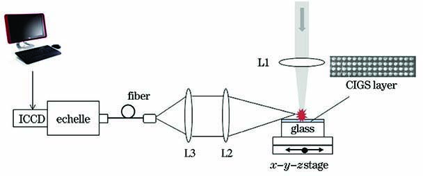
    Fig. 1. LIBS experimental setup for analyzing CIGS thin film
    LIBS spectrum of CIGS thin film
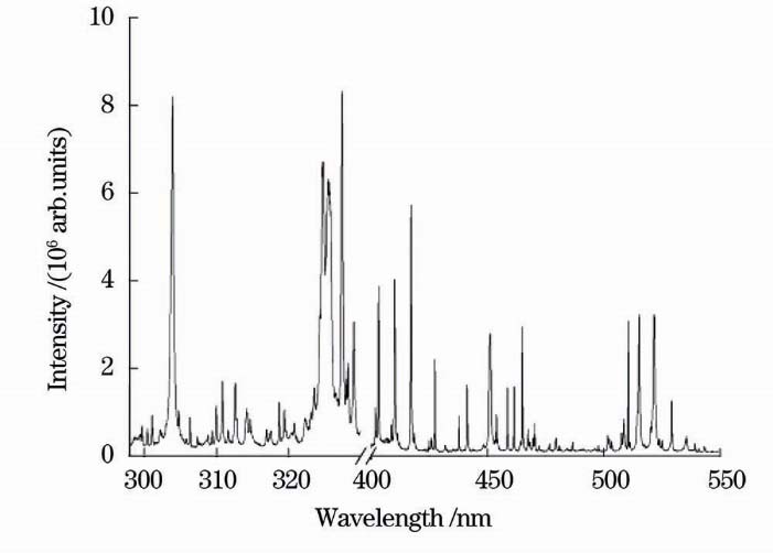
    Fig. 2. LIBS spectrum of CIGS thin film
    Calibration curves of different sample sets. (a) Calibration curves of xGa/x(In+Ga); (b) calibration curves of xCu/x(In+Ga)
    Fig. 3. Calibration curves of different sample sets. (a) Calibration curves of xGa/x(In+Ga); (b) calibration curves of xCu/x(In+Ga)
    Merged calibration curves. (a) Merged calibration curve of xGa/x(In+Ga); (b) merged calibration curve of xCu/x(In+Ga)
    Fig. 4. Merged calibration curves. (a) Merged calibration curve of xGa/x(In+Ga); (b) merged calibration curve of xCu/x(In+Ga)
    EDS and LIBS results of CIGS thin film samples S1, S2 and S3 deposited at different sputtering parameters
    Fig. 5. EDS and LIBS results of CIGS thin film samples S1, S2 and S3 deposited at different sputtering parameters
    Sputtering parameterAtomic concentration ratioSample set
    Power/WPressure/PaTime/minxGa/x(In+Ga)xCu/x(In+Ga)
    901.0100.2980.811F1
    200.2840.842
    300.2750.820
    400.2440.851
    500.2660.882
    900.5600.2730.855F2
    1.00.3200.935
    2.00.3460.990
    2.50.2901.000
    702.0550.2710.976F3
    800.2880.923
    900.3330.944
    950.3210.910
    Table 1. EDS measured xGa/x(In+Ga) and xCu/x(In+Ga) in CIGS thin films obtained at different sputtering parameters
    Atomic concentration ratioFitting equationParameterSingle calibrationMerged calibration
    F1F2F3
    xGa/x(In+Ga)y=a+sxa0.2390.2760.2710.264
    s0.9400.8100.8180.846
    R20.9960.9980.9920.991
    xCu/x(In+Ga)y=a+sx+cx2a0.4600.4380.4410.561
    s0.0310.0560.052-0.206
    c---0.139
    R20.9500.9920.9950.995
    Table 2. Parameters of calibration curves
    SampleSputtering parameterRelative error/%
    Power /WPressure /PaTime /minxGa/x(In+Ga)xCu/x(In+Ga)
    S1851.5352.261.36
    S21001.0454.051.31
    S3651.5251.490.46
    Table 3. Sputtering parameters of three CIGS thin film samples and relative errors between LIBS and EDS results
    Lili Dong, Shiming Liu, Junshan Xiu. Quantitative Analysis of Cu(In,Ga)Se2 Thin Films Deposited by Magnetron Sputtering Technology Using Laser-Induced Breakdown Spectroscopy[J]. Laser & Optoelectronics Progress, 2020, 57(23): 233003
    Download Citation