
Qian Yang, Yongzhou Xue, Hao Chen, Xiuming Dou, Baoquan Sun. Photo-induced doping effect and dynamic process in monolayer MoSe2[J]. Journal of Semiconductors, 2020, 41(8): 082004
- Journal of Semiconductors
- Vol. 41, Issue 8, 082004 (2020)
Abstract
1. Introduction
The monolayer transition metal dichalcogenides (TMDCs) have great potential in the manufacture of optoelectronic devices such as exciton lasers[
In this letter, we report on observations of the laser excitation power dependences of neutral exciton (X) and negatively charged exciton (X–) PL peak intensities at low temperature of 6 K with increasing excitation power from 0.2 to 872 μW, showing a typical irreversible switching over between X and X– PL peak intensities. The dynamic process of the switching over can be described by a power-law distribution of t−α with α = 0.1–0.24, depending on the laser excitation powers. The derived average photo-induced electron transfer time is approximately 27.65 s. As the temperature increases from 20 to 44 K, the energy difference between X and X– shows a downward trend.
2. Experimental section
2.1. Samples and setup
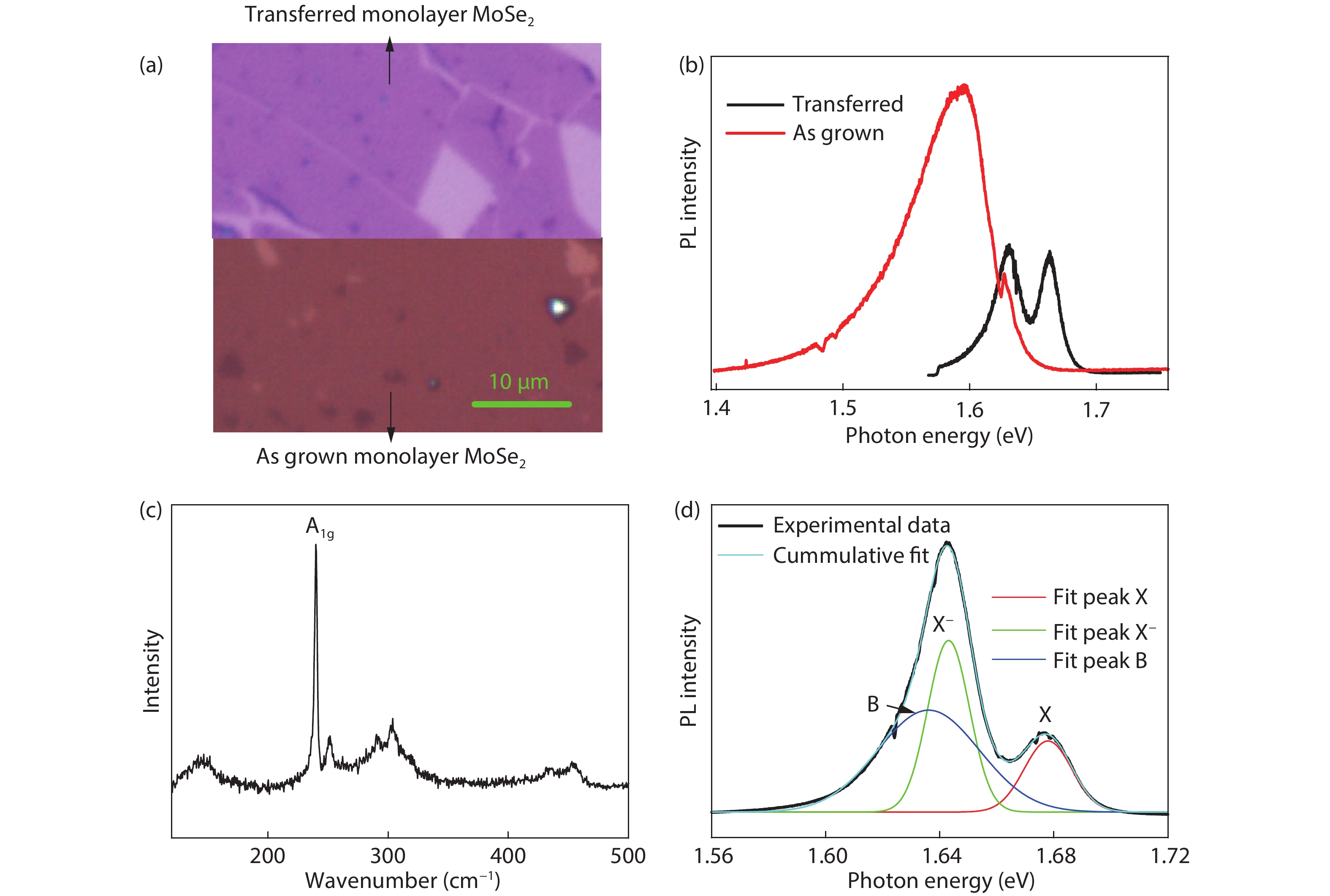
Monolayer MoSe2 sample is grown on a 300 nm SiO2/Si substrate by chemical vapor deposition (CVD) (products by 6 carbon technology). Fig. 1(a) shows the micrographs of the as grown and the transferred monolayer MoSe2 sample, respectively, by 100× objective. Fig. 1(b) shows a typical PL spectrum of the as grown sample measured at 6 K and excitation of 37 μW. Here, owing to a larger lattice mismatch between MoSe2 and substrate as well as a rapid change of the growth temperature[
![]()
Figure 1.(Color online) (a) Micrograph of transferred monolayer MoSe2 sample (upper part) and as grown monolayer MoSe2 sample (lower part). (b) PL spectra of monolayer MoSe2 measured at 6 K for as grown (red line) and after transferring to a SiO2/Si substrate (black line). (c) Raman spectrum of the transferred sample. (d) PL spectrum of the transferred monolayer MoSe2 measured at an excitation power of 872
2.2. Power dependence of MoSe2 photoluminescence
The detailed PL spectra as a function of the excitation power from 0.2 to 872 μW for X and X– emissions are presented in Fig. 2(a), where the PL spectra are measured when the X PL peak intensity become to be steady evidently. As can be seen in Fig. 2(a), when the excitation power is smaller, such as 0.2 μW, X exciton emission is dominant. However, with increasing the excitation power, X– PL peak intensity gradually increases and become to be dominant. Furthermore, X PL peak exhibits a blue-shift, whereas X– PL peak shows a red-shift. Fig. 2(c) summarizes the PL peak shift as a function of the excitation power. Here X PL peak blue-shift and X– PL peak red-shift are attributed to the increase of electron densities[
![]()
Figure 2.(Color online) (a) PL spectra of the transferred monolayer MoSe2 for the first-round measurements with increasing excitation power from 0.2 to 872
In order to further study the power-dependent PL intensity changes of X and X– after the first round laser excitation up to the largest power of 872 μW. We restart to measure the power-dependent PL on the same excitation spot of the sample at 6 K under excitation power from 1 to 760 μW, as shown in Fig. 2(b). It clearly demonstrates that X– PL intensity is always larger than the X, even at the minimum excitation power of 1 μW. Furthermore, it is different from the power-dependence of X and X– characteristics, as shown in Figs. 2(a), 2(c), and 2(e). Here X and X– peak energies, as shown in Fig. 2(d), are basically unchanged with increasing the excitation power, and the PL peak intensities have nearly the same rate of increase, as shown in Fig. 2(f). For the second-round power changing measurements, the X– emission is dominant even at the minimum excitation power after the sample is irradiated by large laser power. This implies that in both round measurements, the equilibrium state of the conduction band is different. In the first round, the conduction band has no electrons, while the second round has redundant electrons. This phenomenon has been reported and is interpreted by photo-doping effect[
2.3. Time-resolved measurements
To study the dynamics of photo-induced electrons, the time evolution of X PL peak intensity is measured by using a modulated cw laser excitation. Here AOM is used as a fast switch of the cw laser. In the experiment, as soon as the laser is turned on, the X PL peak intensity is detected by an APD and the time evolution is recorded by an MCS with a time bin of 100 ms and time range of 60 s. The recorded data are plotted in Fig. 3(a) under different laser excitation powers, where the ordinate is logarithmic and the curves of different powers are shifted relatively for clarity. It is found that for the excitation power ranges from 0.5 to 100 μW, the decay law of X PL peak intensity can be described by power-law distribution of
![]()
Figure 3.(Color online) (a) PL intensity of X as a function of time measured by a modulated cw laser excitation with power from 0.5 to 100
As can be seen in Figs. 3(c) and 3(d), as time increases, a change of the X PL peak intensity can be fitted by power-law function. Assuming that the total PL intensity of X and X– remains constant at a fixed excitation power, the decrease of the X PL intensity with time delay implies that more electrons transfer into X– energy level which is lower than X. This results in an increase of X– PL intensity. Then the average electron transfer time < t> from X to X– band can be obtained with power-law distribution. Here the luminescence intensity
Thus the average electron transfer time based on of Eq. (1) is:
Based on the experimental curves as shown in Fig. 3(a), we can calculate the numerical integral of the denominator of Eq. (2)[
2.4. Temperature dependence of MoSe2 photoluminescence
In order to obtain a stable spectrum in a short time, the laser power is first set to 118 μW to irradiate the sample, and then the power is kept at 42 μW for temperature dependent PL measurements. As shown in Fig. 4(a), when T < 15 K, it can be found that the PL intensity of the monolayer MoSe 2 sample keep almost unchanged. In the range of 20 K < T < 40 K, the temperature is increased slowly at 1 K intervals, the intensity of X is relatively stable, and the intensity of X – decreases evenly with the increase of temperature. As shown in inset of Fig. 4(a), the ratio of PL peak intensity of X– and X shows a good negative linear law with temperature, and the linear fitting slope is obtained to be –0.07. The energy difference between the two peaks shows a downward trend as the temperature increases from 20 to 44 K (Fig. 4(b)). They imply that the increasing of temperature (20–40 K) may have a negative influence on the photo doping effect in monolayer MoSe2.
![]()
Figure 4.(Color online) (a) The PL spectra of the transferred monolayer MoSe2 with the temperature increased from 6 to 44 K, under the 42
3. Conclusion
In summary, we have studied the excitation power dependence of the X and X– PL intensities for the transferred monolayer MoSe2 at 6 K. When the laser excites the sample with a power of tens of μW, an irreversible switching over between X and X– PL peak intensities occurs. After laser irradiation, X– emission will be dominated even if the excitation power is reduced by less than μW. This indicates the generation of additional electrons by optical excitation or photodoping process. Dynamic process of electron transfer can be described by power-law distribution t−α with α = 0.1–0.24 depending on the laser excitation powers. The obtained average electron transfer time is approximately 27.65 s. In the temperature range of 20 < T < 44 K, the increase of temperature induces the reduction of the ratio of the PL peak intensity of X – and X, also, the reduction of the two peak energy difference. The photodoping effect provides a convenient way of local doping of electrons, which may be useful for new device fabrication.
Acknowledgements
This work was supported by the National Natural Science Foundation of China under Grant Nos 61674135, 11974342 and 61827823.
References
[1] O Salehzadeh, M Djavid, N H Tran et al. Optically pumped two-dimensional MoS2 lasers operating at room-temperature. Nano Lett, 15, 5302(2015).
[2] Y Ye, Z J Wong, X F Lu et al. Monolayer excitonic laser. Nat Photon, 9, 733(2015).
[3] S Wu, S Buckley, J R Schaibley et al. Monolayer semiconductor nanocavity lasers with ultralow thresholds. Nature, 520, 69(2015).
[4] A Pospischil, M M Furchi, T Mueller. Solar-energy conversion and light emission in an atomic monolayer p–n diode. Nat Nanotechnol, 9, 257(2014).
[5] F Withers, O del Pozo-Zamudio, A Mishchenko et al. Light-emitting diodes by band-structure engineering in van der Waals heterostructures. Nat Mater, 14, 301(2015).
[6] M Koperski, K Nogajewski, A Arora et al. Single photon emitters in exfoliated WSe2 structures. Nat Nanotechnol, 10, 503(2015).
[7] Y M He, G Clark, J R Schaibley et al. Single quantum emitters in monolayer semiconductors. Nat Nanotechnol, 10, 497(2015).
[8] R Roldán, J A Silva-Guillén, M P López-Sancho et al. Electronic properties of single-layer and multilayer transition metal dichalcogenides MX2 (M = Mo, W and X = S, Se). Ann Der Physik, 526, 347(2014).
[9] M Currie, A T Hanbicki, G Kioseoglou et al. Optical control of charged exciton states in tungsten disulfide. Appl Phys Lett, 106, 201907(2015).
[10] A Singh, G Moody, K Tran et al. Trion formation dynamics in monolayer transition metal dichalcogenides. Phys Rev B, 93, 041401(2016).
[11] T Godde, D Schmidt, J Schmutzler et al. Exciton and trion dynamics in atomically thin MoSe2 and WSe2: Effect of localization. Phys Rev B, 94, 165301(2016).
[12] T Liu, D Xiang, Y Zheng et al. Nonvolatile and programmable photodoping in MoTe2 for photoresist-free complementary electronic devices. Adv Mater, 30, 1804470(2018).
[13] J Quereda, T S Ghiasi, C H van der Wal et al. Semiconductor channel-mediated photodoping in h-BN encapsulated monolayer MoSe2 phototransistors. 2D Mater, 6, 025040(2019).
[14] J S Ross, S F Wu, H Y Yu et al. Electrical control of neutral and charged excitons in a monolayer semiconductor. Nat Commun, 4, 1474(2013).
[15] F Cadiz, C Robert, G Wang et al. Ultra-low power threshold for laser induced changes in optical properties of 2D molybdenum dichalcogenides. 2D Mater, 3, 045008(2016).
[16] P Atkin, D M Lau, Q Zhang et al. Laser exposure induced alteration of WS2 monolayers in the presence of ambient moisture. 2D Mater, 5, 015013(2017).
[17] Z Liu, M Amani, S Najmaei et al. Strain and structure heterogeneity in MoS2 atomic layers grown by chemical vapour deposition. Nat Commun, 5, 5246(2014).
[18] X Fu, F Li, J F Lin et al. Pressure-dependent light emission of charged and neutral excitons in monolayer MoSe2. J Phys Chem Lett, 8, 3556(2017).
[19] J Pei, J Yang, X Wang et al. Excited state biexcitons in atomically thin MoSe2. ACS Nano, 11, 7468(2017).
[20] N Lundt, E Cherotchenko, O Iff et al. The interplay between excitons and trions in a monolayer of MoSe2. Appl Phys Lett, 112, 031107(2018).
[21]
[22] H Scher, E W Montroll. Anomalous transit-time dispersion in amorphous solids. Phys Rev B, 12, 2455(1975).
[23] J Kakalios, R A Street, n W B Jackson. Stretched-exponential relaxation arising from dispersive diffusion of hydrogen in amorphous silicon. Phys Rev Lett, 59, 1037(1987).

Set citation alerts for the article
Please enter your email address
© Copyright 2018-2021 | Chinese Laser Press. All Rights Reserved 沪ICP备15018463号-20