• Journal of Infrared and Millimeter Waves
  • Vol. 40, Issue 3, 308 (2021)
Wei-Ting ZHANG1、2, Xing CHEN1, and Zhen-Hua YE1、*
Author Affiliations
  • 1Key Laboratory of Infrared Imaging Materials and Devices, Shanghai Institute of Technical Physics, Chinese Academy of Sciences, Shanghai 200083, China
  • 2University of Chinese Academy of Sciences, Beijing 100049, China
  • show less
    DOI: 10.11972/j.issn.1001-9014.2021.03.005 Cite this Article
    Wei-Ting ZHANG, Xing CHEN, Zhen-Hua YE. Stress in HgCdTe large infrared focal plane array detector analyzed with finite element analysis[J]. Journal of Infrared and Millimeter Waves, 2021, 40(3): 308 Copy Citation Text show less
    Three-dimensional structure diagram of the detector
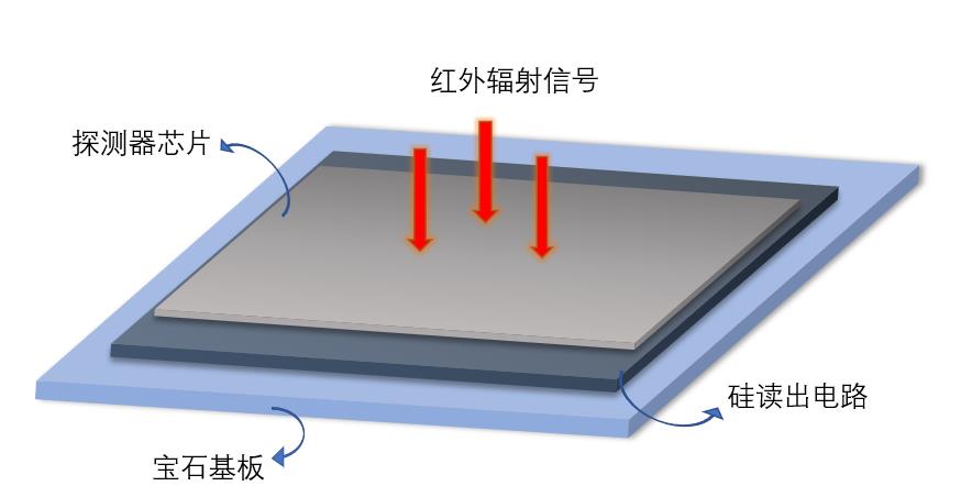
    Fig. 1. Three-dimensional structure diagram of the detector
    Detector profile with Kovar equilibrium layer
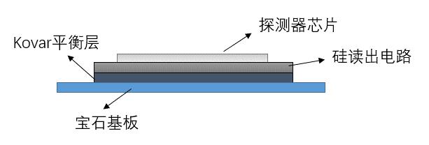
    Fig. 2. Detector profile with Kovar equilibrium layer
    Multi-layer material structure system
    Fig. 3. Multi-layer material structure system
    Warpage deformation of multi-layer material system
    Fig. 4. Warpage deformation of multi-layer material system
    Finite element mesh of module
    Fig. 5. Finite element mesh of module
    Without Kovar equilibrium layer (a) thermal deformation in low temperature, (b) thermal stress (z-axis downward is positive direction)
    Fig. 6. Without Kovar equilibrium layer (a) thermal deformation in low temperature, (b) thermal stress (z-axis downward is positive direction)
    With Kovar equilibrium layer (a) thermal deformation in low temperature; (b) thermal stress (z-axis downward is positive direction)
    Fig. 7. With Kovar equilibrium layer (a) thermal deformation in low temperature; (b) thermal stress (z-axis downward is positive direction)
    Material layers composition of detector chip
    Fig. 8. Material layers composition of detector chip
    Comparison between adding Kovar equilibrium layer and not adding Kovar equilibrium layer (a) epilayer thermal stress of HgCdTe detector, (b) low temperature deformation of the centerline of detector chip surface
    Fig. 9. Comparison between adding Kovar equilibrium layer and not adding Kovar equilibrium layer (a) epilayer thermal stress of HgCdTe detector, (b) low temperature deformation of the centerline of detector chip surface
    On the detector chip (a) the curve of maximum thermal stress changing with thickness of Kovar equilibrium layer; (b) the curve of the deformation changing with the thickness of Kovar equilibrium layer
    Fig. 10. On the detector chip (a) the curve of maximum thermal stress changing with thickness of Kovar equilibrium layer; (b) the curve of the deformation changing with the thickness of Kovar equilibrium layer
    结构名称
    GaAs衬底36.8 mm36.8 mm0.65 mm
    HgCdTe36.8 mm36.8 mm0.01 mm
    硅读出电路40.3 mm39.1 mm0.48 mm
    Kovar平衡层40.3 mm39.1 mm1 mm
    宝石基板43 mm45.2 mm0.33 mm
    Table 1. Material dimension parameters
    材料名称泊松比平均弹性模量/GPa平均线膨胀系数/ppm/K
    砷化镓0.31904.55
    0.281301.15
    宝石基板0.253903.15
    碲镉汞0.3604.62
    可伐0.32006.5
    Table 2. Material properties
    Wei-Ting ZHANG, Xing CHEN, Zhen-Hua YE. Stress in HgCdTe large infrared focal plane array detector analyzed with finite element analysis[J]. Journal of Infrared and Millimeter Waves, 2021, 40(3): 308
    Download Citation