1Huazhong University of Science and Technology, Wuhan National Laboratory for Optoelectronics and School of Optical and Electronic Information, Wuhan, China
2China Information and Communication Technologies Group Corporation, State Key Laboratory of Optical Communication Technologies and Networks, Wuhan, China
3National Information Optoelectronics Innovation Center, Wuhan, China
Parity‐time (PT) symmetry breaking offers mode selection capability for facilitating single‐mode oscillation in the optoelectronic oscillator (OEO) loop. However, most OEO implementations depend on discrete devices, which impedes proliferation due to size, weight, power consumption, and cost. In this work, we propose and experimentally demonstrate an on-chip tunable PT‐symmetric OEO. A tunable microwave photonic filter, a PT‐symmetric mode‐selective architecture, and two photodetectors are integrated on a silicon‐on‐insulator chip. By exploiting an on‐chip Mach–Zehnder interferometer to match the gain and loss of two mutually coupled optoelectronic loops, single‐mode oscillation can be obtained. In the experiment, the oscillation frequency of the on-chip tunable PT‐symmetric OEO can be tuned from 0 to 20 GHz. To emulate the integrated case, the OEO loop length is minimized, and no extra-long fiber is used in the experiment. When the oscillation frequency is 13.67 GHz, the single‐sideband phase noise at 10-kHz offset frequency is -80.96 dBc / Hz and the side mode suppression ratio is 46 dB. The proposed on-chip tunable PT‐symmetric OEO significantly reduces the footprint of the system and enhances mode selection.
The high‐quality microwave signal is the cornerstone of many application fields such as radar, wireless communication, and electronic warfare systems.1,2 The optoelectronic oscillator (OEO) has been considered an effective method to generate microwave signals with low phase noise at high frequency.3 The high‐quality factor of the OEO cavity is ensured by the long and low‐loss optical fiber, which guarantees low phase noise but makes mode selection difficult, due to the ultranarrow eigenmode frequency spacing.4,5 In a traditional OEO, an electrical bandpass filter (EBF) is used for mode selection. However, the center frequency of the EBF is usually fixed or can only be tuned within a small frequency range.6–8 Hence, the frequency tunability of EBF‐based OEO is extremely limited.8 By contrast, the microwave photonic filter (MPF) is advantageous in wideband tunability.9 Therefore, the oscillation frequency of the MPF‐based OEO can be widely tuned.10–12 For example, a widely tunable OEO has been realized by using an MPF based on a phase‐shifted fiber Bragg grating (PS‐FBG),10 a microdisk resonator (MDR),11 or the stimulated Brillouin scattering (SBS) effect in the high nonlinear fiber.12 Notably, the mode selection of the OEO is limited by the bandwidth of the MPF. To enhance mode selection, an MPF with ultranarrow bandwidth is desired.
Recently, parity‐time (PT) symmetry breaking has been proven as a powerful mode selection mechanism to achieve single‐mode oscillation.13–18 In a spatial PT‐symmetric OEO, two mutually coupled optoelectronic feedback loops are identical in geometry, but one experiences gain while the other experiences an equal amount of loss. To ensure that PT symmetry is successfully established to perform mode selection, the geometry of the two coupled loops must be perfectly matched and the gain, loss, and coupling coefficients between the two coupled loops can be manipulated. When the gain/loss is larger than the coupling coefficient, the PT symmetry is broken. PT-symmetry breaking is critical to ensure single‐mode oscillation, which enlarges the gain difference between the dominant oscillation mode and other modes. PT‐symmetric OEO with a single spatial loop has also been demonstrated in wavelength space. However, two tunable laser sources (TLSs) are required, and the frequency of the generated microwave signal is fixed.18 Nevertheless, PT-symmetric OEOs mentioned above are constructed based on discrete devices, and suffer from being bulky systems, having high costs, and being sensitive to environmental fluctuations.13–17 Specifically, the photonic integrated circuits (PICs) pave the way for the emerging integrated microwave photonics (IMWP). The IMWP is superior in size, weight, power, and cost (SWaP‐C).19–22 Thus, miniaturization and integration of the OEO is an essential step towards practical applications and commercialization. Among the available integrated material platforms, silicon photonics has been attracting intense interest because of its intrinsic advantages, such as low cost, large refractive contrast, and compatibility with the mature complementary metal oxide semiconductor (CMOS) technology.22
In this work, we propose and experimentally demonstrate an on-chip tunable PT‐symmetric OEO based on a silicon‐on‐insulator (SOI) wafer. A high‐Q microring resonator (MRR), a PT‐symmetric mode‐selective architecture, and two high‐speed photodetectors (PDs) are integrated on the silicon platform, which significantly reduces the footprint of the PT-symmetric OEO. The on‐chip PT‐symmetric mode‐selecting architecture consists of a tunable Mach–Zehnder interferometer (MZI) and two waveguides with equal lengths. By adjusting the phase difference of two arms in the MZI, gain and loss can be controlled to achieve stable single‐mode oscillation. The on-chip PT-symmetric mode-selecting architecture is more robust than the discrete one, and the complexity of the system is simplified by eliminating the external tunable delay line, which ensures that the loop lengths of the two mutually coupled loops are equal. Meanwhile, an MRR‐based MPF is also incorporated in the OEO cavity to adjust the oscillation frequency of the OEO. The combination of high‐quality MPF and PT symmetry can significantly enhance mode selection and make the OEO tunable. In the experiment, the generated microwave signal can be tuned from 0 to 20 GHz by adjusting the center frequency of the MPF. When the frequencies of the generated microwave signal are tuned to 4.97 and 13.67 GHz, the measured single sideband (SSB) phase noises at 10-kHz offset frequency are and , respectively. The proposed PT‐symmetric OEO explores an effective solution for mode selection and dramatically accelerates the development of monolithically integrated OEO.
Sign up for Advanced Photonics Nexus TOC. Get the latest issue of Advanced Photonics Nexus delivered right to you!Sign up now
2 Principle
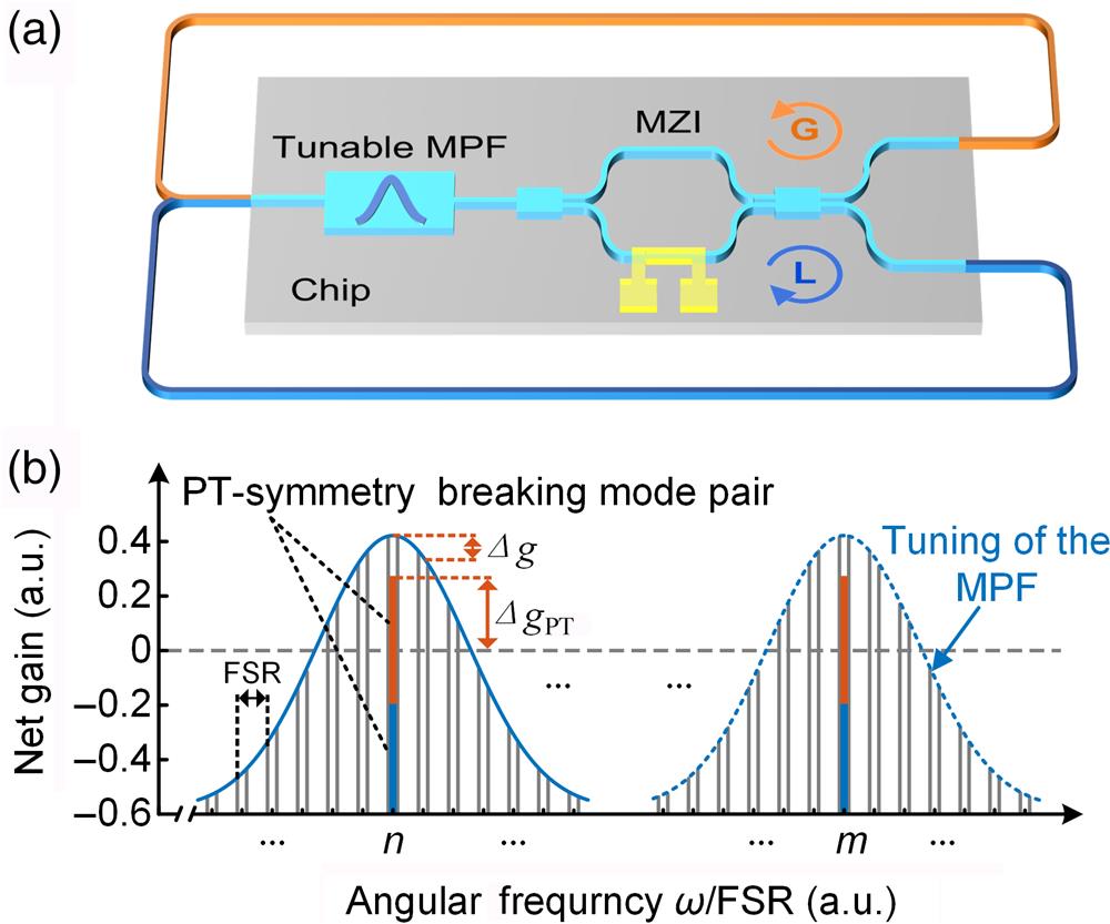
The schematic diagram of the on-chip tunable PT‐symmetric OEO is shown in Fig. 1(a). An integrated tunable MPF is established for coarse mode selection and tunability. Note that the bandwidth of the MPF should be as narrow as possible to ensure single-mode oscillation. However, in actual operation, the bandwidth is usually not narrow enough, and multimode oscillation exists. To ensure single-mode oscillation, an integrated PT‐symmetric mode‐selective architecture is subsequently constructed. As shown in Fig. 1(a), the tunable PT‐symmetric OEO consists of two mutually coupled feedback loops with the same free spectral range (FSR) but opposite round‐trip gain. Gain and loss can be controlled accurately by adjusting the voltage applied to the microheater on one branch of the MZI. Theoretically, the coupled differential equations of the ’th oscillation mode in two mutually coupled loops can be expressed as13,14where and are the amplitudes of the ’th oscillation mode in the two loops, is the angular frequency of the ’th oscillation mode in the two loops, is the coupling coefficient between the gain and loss loops for the ’th oscillation mode, and and are the gain and loss coefficients of the gain and loss loops for the ’th oscillation mode, respectively.
Figure 1.(a) Schematic diagram and (b) mode selection principle of the on-chip tunable PT‐symmetric OEO. MPF, microwave photonic filter; MZI, Mach–Zehnder interferometer; FSR, free spectral range.
By solving Eq. (1), the eigenfrequencies of the ’th oscillation mode in the OEO loop can be derived as Under PT symmetry, it is required that the gain and loss coefficients of both cross‐coupled loops are equal in magnitude, i.e., . Therefore, Eq. (2) can be simplified as It can be obtained from Eq. (3) that PT symmetry exhibits two distinctly different phases by manipulating the gain, loss, and coupling coefficients between the two coupling loops. When the gain coefficient is smaller than the coupling coefficient (), any pair of modes remains neutral and the eigenfrequency remains nondegenerate. Assume that the ’th mode has the largest gain, which is determined by the amplitude frequency response of the MPF [see Fig. 1(b), blue solid curve]. When only the gain coefficient of the ’th mode is larger than the coupling coefficient (), the PT symmetry of the ’th mode is broken, and a conjugate pair of amplifying and decaying eigenmodes is generated. Meanwhile, the other modes except the ’th mode remain in PT symmetry because of undergoing smaller gain. Hence, the amplifying mode obtains a much higher gain against the other modes and enables stable oscillation, as shown in Fig. 1(b). Notably, when the center frequency of the MPF is tuned to be aligned with the ’th mode of the OEO [see Fig. 1(b), blue dashed curve], the PT symmetry of the ’th mode is then broken. As a result, the ’th mode achieves single-mode oscillation, and the oscillation frequency of OEO is tuned.
Generally, a traditional single‐loop OEO to achieve single‐mode oscillation requires that the net gain of the dominant oscillation mode is above zero while the others are below zero. As depicted in Fig. 1(b), the gain difference between the dominant oscillation mode (’th mode) and the secondary mode [()’th mode] with the second highest gain in a traditional single‐loop OEO can be expressed as Obviously, it is difficult to obtain stable single‐mode oscillation because of the small gain difference, especially with narrow mode spacing. In a PT‐symmetric OEO, assuming that the secondary mode satisfies the critical condition of PT-symmetry breaking, the gain difference between the dominant oscillation mode and the secondary mode can be expressed as Combining Eqs. (4) and (5), the gain enhancement factor can be expressed as In an OEO with small mode spacing, we have . Hence, a larger gain difference is obtained, and the mode selection is significantly enhanced, as indicated by Eq. (6). Consequently, in our proposed scheme, the MPF and PT symmetry cooperate to render the OEO stable single‐mode oscillation and frequency tunability.
3 Results
3.1 Chip Design and Fabrication
According to the theoretical analysis, the chip shown in Fig. 2(a) is designed to realize tunable PT‐symmetric OEO. A grating coupler (GC) array is used to couple the optical signal into and out of the chip simultaneously, and the GCs are uniformly placed with a center spacing of . The optical signal is coupled into the chip through and then processed by an all‐pass high-Q MRR. Then the optical signal is equally divided into the two branches of the MZI by a multimode interferometer (). The microheater on the lower branch of the MZI is used to control the power splitting ratio between the two outputs of the . Finally, the optical signals from the two outputs of the are injected into two identical high‐speed silicon‐germanium (Si‐Ge) PDs to recover microwave signals. Here, several test ports are reserved for monitoring the operation state of the chip. The PIC shown in Fig. 2(a) performs the functions of frequency tuning, mode selection, and optical‐to‐electrical conversion.
The designed chip is fabricated on an SOI wafer with a buried oxide layer and a 220‐nm top Si layer. The packaged chip is shown in Fig. 2(b). The chip is glued on the printed circuit board (PCB) and an optical fiber array (FA) is glued to the grating array to perform vertical coupling. The direct current (DC) electrodes on the chip are connected to the PCB by wire bonding. Figure 2(c) shows the micrograph image of the fabricated device with false color. A high-Q MRR, an MZI, and two PDs are integrated on the same chip. The inset in Fig. 2(c) shows the zoom‐in views of the coupling region of the MRR, MZI, and the two PDs. The high-Q MRR is fabricated to implement a tunable MPF, which is used to perform coarse mode selection. To attain a narrower bandwidth of MPF, the MRR structure is designed as shown in the inset in Fig. 2(a). The MRR consists of two half-rings, two straight waveguides, and four connecting adiabatic tapers. To prevent exciting the high-order modes, a single-mode waveguide with 500-nm width is used in both the bus waveguide and the half-rings. The gap between the bus waveguide and the MRR is 460 nm, and the MRR is under-coupled. The width of the two straight waveguides is designed to be for reducing the surface scattering losses caused by sidewall roughness.23 The single-mode and multimode waveguides are connected by a linear adiabatic taper. Meanwhile, the whole chip is designed as a ridge waveguide, which can further reduce the transmission loss. The FSR of the MRR is 0.33 nm, corresponding to 41.25 GHz. To accurately characterize the bandwidth of the MRR, a vector network analyzer (VNA, Anritsu, MS4647B) is used to measure the amplitude frequency response of the MRR‐based MPF, as shown in Fig. 2(d). The measured full width at half‐maximum (FWHM) bandwidth is 187 MHz, indicating that the loaded quality factor of the MRR is . Additionally, the high‐speed PD with a responsivity of is used to recover the electrical signal. Figure 2(e) shows the frequency response of the PD at a reverse‐biased voltage of 3 V, and it can be seen that the FWHM bandwidth of the PD is 33 GHz. In addition, the measured optical insertion loss of the chip is 14.64 dB, including the coupling grating loss of 4.94 dB, the splitting loss of 9 dB of three MMIs, and the link propagation loss of 0.7 dB.
Figure 2.Tunable PT-symmetric OEO chip. (a) Schematic diagrams of the designed Si photonic chip and MRR; (b) image of the packaged chip; (c) micrograph of the fabricated chip with false color. The inset is a zoomed-in view of key components: ① coupling region of the MRR, ② MZI, and ③ two PDs. (d) Measured amplitude frequency response of the MRR-based MPF. The inset is the zoomed-in view of the microwave passband. (e) Measured frequency response of the PD. GC, grating coupler; MMI, multimode interferometer; MRR, microring resonator; PD, photodetector; PCB, printed circuit board.
3.2 Results of the On-Chip Tunable PT-Symmetric OEO
To investigate the performance of the on-chip tunable PT‐symmetric OEO, an experimental setup as shown in Fig. 3(a) is performed. A continuous wave (CW) light emitted from a TLS (NKT Basik E15) is sent to a phase modulator (PM, Covega Mach‐40) via a polarization controller (), which is used to adjust the state of polarization (SOP) of the optical carrier. The erbium‐doped fiber amplifier (EDFA) is used to amplify the phase‐modulated signal. Then the SOP of the phase‐modulated signal is adjusted by and injected into the chip via the . The phase‐modulated signal is transmitted through a high-Q MRR to achieve phase‐modulation to intensity‐modulation (PM‐IM) conversion. Next, the optical signal passes through the PT‐symmetric mode‐selection architecture for a precise mode selection. The optical signals are converted into two microwave signals and then combined by an electrical combiner (EC). Finally, the microwave signal is amplified by electrical amplifiers (EAs, SHF S824A, SHF S804A, and SHF S804B) and fed back to the PM to form a closed OEO loop. The electrical spectrum and phase noise of the generated microwave signals are measured by a phase noise analyzer (ROHDE&SCHWARZ FSWP).
Figure 3.(a) Experimental setup of the tunable PT‐symmetric OEO; (b) measured open‐loop amplitude frequency response of the tunable PT‐symmetric OEO. The inset shows the comparison between the zoomed‐in views of the open‐loop gain spectrum (blue solid curve) and the gain spectrum under PT-symmetry breaking (red dashed curve). (c) When only the MPF is applied to the OEO, the measured electrical spectrum has a span of 1 GHz and an RBW of 3 MHz. The inset shows a zoomed‐in view of the electrical spectrum with a span of 20 MHz and an RBW of 50 kHz. (d) When the MPF and PT-symmetry breaking are combined to be used in the OEO, the measured electrical spectrum has a span of 1 GHz and an RBW of 3 MHz. The inset shows a zoomed‐in view of the electrical spectrum with a span of 100 MHz and an RBW of 300 kHz. (e) The electrical spectra of single‐mode oscillation (blue solid curve) and multimode oscillation (red dashed curve) with a span of 10 MHz and an RBW of 50 kHz. TLS, tunable laser source; PC, polarization controller; PM, phase modulator; EDFA, erbium doped fiber amplifier; DUT, device under test; EC, electrical combiner; EA, electrical amplifier; PS, power splitter; ESA, electrical spectrum analyzer.
In the proposed OEO, by adjusting the DC voltage on the microheater on the branch of the MZI, gain and loss can be accurately controlled. The gain and loss coefficients can be expressed as (see Appendix) where is the maximal round‐trip gain of the proposed PT‐symmetric OEO at the center frequency of the MPF, is the phase shift of the optical signal in one branch of the MZI, and is the round‐trip time of the proposed OEO. Based on Eqs. (7) and (8), the phase shift under PT symmetry satisfies As can be seen, the PT symmetry can be achieved by adjusting the phase shift of one branch of the MZI when is larger than 2.
In the experiment, the open‐loop amplitude frequency response of the on-chip tunable PT‐symmetric OEO is measured by a VNA at first. To measure the open‐loop amplitude response when only the MPF is used in the OEO, the MZI should be adjusted to make all of the optical power output at one port of the . Therefore, only one PD receives all of the optical signal and the other PD does not work. Consequently, the open‐loop amplitude response can be obtained. In the experiment, when the voltage applied to the MZI is 3.1 V, the optical power injected into gets its maximal value 1.52 dBm. Meanwhile, the optical power injected into is , which is too low to be detected by . Consequently, the measured open‐loop amplitude frequency response is shown in Fig. 3(b). Notably, the optical power applied to and is monitored by and , respectively. When the OEO loop is closed, the measured electrical spectrum of the OEO with a center frequency of 13.67 GHz is shown in Fig. 3(c). The inset in Fig. 3(c) is a zoomed‐in view of the electrical spectrum, which clearly indicates that multimode oscillation is happening. The mode spacing of the OEO loop is 4 MHz and the corresponding loop length is calculated to be 50 m, including 33-m optical fiber in the EDFA, 12.5-m optical fiber pigtails of the devices, 1 m optical coupling fiber for device under test (DUT) coupling, and 3.5-m radio-frequency cables. Ideally, the optical circuit, and even the electrical circuit of the PT-symmetric OEO would be fully integrated. Therefore, to emulate the full integration case, no extra-long optical fiber, which can serve to further reduce phase noise, is utilized in the experiment. Adjusting the voltage applied to the MZI, the gain and loss can be balanced and PT-symmetry breaking can be obtained. The inset in Fig. 3(b) shows the comparison between the open‐loop amplitude responses without and with PT-symmetry breaking. Assuming the gain of the dominant oscillation mode remains invariant, the amplitude responses without and with PT-symmetry breaking are shown as the blue solid curve and the red dashed curve, respectively. The amplitude response with PT-symmetry breaking is derived based on the measured amplitude frequency response (blue solid curve) and Eq. (5). It can be observed that the gain difference between the dominant oscillation mode and the other modes is significantly enlarged by PT-symmetry breaking. When the voltage applied to the microheater on the MZI is 1.8 V, the measured electrical spectrum centered at 13.67 GHz is shown in Fig. 3(d). The inset in Fig. 3(d) shows the electrical spectrum with a span of 100 MHz and a resolution bandwidth (RBW) of 300 kHz. Therefore, when the PT-symmetry breaking is incorporated into the OEO loop, single-mode oscillation is obtained, and the side mode suppression ratio (SMSR) exceeds 45 dB. Figure 3(e) shows the comparison between the electrical spectra of single‐mode and multimode oscillations with a span of 10 MHz and an RBW of 50 kHz. It is distinctly noted that the power of the dominant oscillation mode is increased by 2.6 dB, while the power of the two adjacent side modes is suppressed by 37.6 and 40 dB under the PT-symmetry breaking, respectively. Here, the suppression ratio between the oscillation mode and the right-hand side mode is 46 dB.
Notably, the frequency of the generated microwave signal can be tuned by adjusting the center frequency of the MPF. In the experiment, the oscillation frequency is tuned from 0 to 20 GHz by adjusting the laser wavelength, and the tuning range is limited by the FSR of the MRR. Especially, the high‐order harmonics can be observed in Fig. 4(a). The high-order harmonics originate essentially from the nonlinearity in the OEO loop.11,12 In our proposed PT-symmetric OEO, the high-order harmonics are mainly caused by the three cascaded electrical amplifiers. As mentioned in Section 3.1, the integrated photonic chip is designed with multiple test ports to monitor the optical power during the experiment. These test ports induce an optical loss of 9 dB, which corresponds to a microwave loss of 18 dB.4 Hence, three cascaded EAs are required in the OEO loop to compensate for the large loop loss, and harmonics are generated. However, in practice, these test ports can be eliminated, and the number of adopted EAs can be reduced. Consequently, the power of the high-order harmonics can be reduced. Further, the power of the high-order harmonics can be further reduced by employing devices with lower nonlinear efficiencies. Figure 4(b) shows the measured phase noises of the microwave signals generated at 4.97 (red dashed curve) and 13.67 GHz (blue solid curve), respectively. As can be seen, the corresponding SSB phase noises at 10-kHz offset frequency are and , respectively. A slight degradation of the phase noise at 13.67 GHz can be observed, which can be blamed on the performance degradation of the electrical devices at high frequency.24,25 The parasitic noise peaks at the 84-kHz offset frequency and its harmonics are induced by cascaded EAs.24,26 Additionally, the stability of the oscillation frequency is measured by using the Maxhold function of the ESA, as shown in Fig. 4(c). It can be observed that the frequency drift is 324.4 kHz in 1 min when the oscillation frequency is 3.52 GHz. The frequency shift is mainly attributed to the drift of the MRR resonant wavelength, which is affected by on-chip thermal cross talk and environmental perturbations. To suppress the thermal cross talk, the thermal isolation trenches could be set around the waveguides of the MRR and the MZI.27 In addition, these devices could be placed in antivibration, constant temperature condition to mitigate the influence of environmental perturbations. Additionally, for long-term stability of the OEO, the thermoelectric cooler (TEC) and the feedback control loop can be exploited to ensure the stability of the output frequency.
Figure 4.(a) Frequency tunability of the proposed PT-symmetric OEO; (b) measured phase noises when the oscillation frequencies are 4.97 GHz (red dashed curve) and 13.67 GHz (blue solid curve), respectively; (c) measured frequency drift within 1 min at an oscillation frequency of 3.52 GHz.
A comparison of previously reported representative OEOs with this work is shown in Table 1. It can be observed that the phase noises of integrated OEOs are higher than that of fiber-based OEOs, which are attributed to the small time delay in the OEO loops. This problem can be solved by further boosting the Q factor of the microresonator in the integrated OEO. Therefore, the waveguide propagation loss should be further reduced by optimizing the design of the high-Q MRR31,32 or by thermal oxidation of the Si waveguides.33 Moreover, a fully integrated OEO, converging optical and electrical circuits, aims to develop chip-scale microwave photonic systems for generating microwave signals with low phase noise and wideband tunability. Therefore, the SWaP-C can be significantly reduced. In OEO, the loss of the overall link is critical. It is worth noting that an EDFA is used in the experiments to compensate for the optical losses. In the future, the EDFA can be removed by further eliminating the test ports, which is also helpful in improving phase noise. Additionally, heterogeneous integration is a promising candidate to harness the unique advantages of different material platforms to provide photonic components functionality, which could further enhance the performance and compactness of the system, for example, low-noise lasers based on indium phosphide and silicon nitride (InP-),34 large-bandwidth electro-optical modulators based on thin-film lithium niobate (),35 ultra-high Q resonators based on silicon nitride (),36 high-speed and high-power germanium (Ge) PD.37 In addition, Si photonics offers compatibility with CMOS technology, and the electrical components in the OEO, including the EA, EC, and power splitter (PS), can be monolithically integrated into the chip.38,39 By doing so, a fully monolithically integrated OEO with low phase noise can be achieved.
Architecture
Mode selection
Tunability
Phase noise (dBc/Hz)
Monolithic integration
Single-loop OEO (16 km)28
EBF
Fixed (10 GHz)
−163 (@6 kHz)
No
Dual-loop OEO (2 km)5
Vernier Effect + EBF
Fixed (10 GHz)
−140 (@10 kHz)
No
Coupled OEO (800 m)6
Vernier Effect + EBF
Fixed (10 GHz)
−110 (@10 kHz)
No
MPF-based OEO (1 km)12
SBS-MPF + IIR-MPF
0–40 GHz
−113 (@10 kHz)
No
PT-symmetric OEO (3.2 km)13
PT Symmetry
Fixed (4 GHz)
−139 (@10 kHz)
No
InP-based PT-symmetric OEO (5 km)29
PT Symmetry
24–25 GHz
−108 (@10 kHz)
Yes
WGMR-based OEO3
High-Q WGMR
Fixed (30 GHz)
−108 (@10 kHz)
No
Chalcogenide-based OEO30
SBS-MPF
5–40 GHz
−100 (@100 kHz)
Yes
InP-based Integrated OEO20
EBF
8.86–8.88 GHz
−92 (@1 kHz)
Yes
Partial silicon-based OEO21
MDR-MPF
3–8 GHz
−80 (@10 kHz)
Yes
This work
MRR-MPF + PT Symmetry
0–20 GHz
−83.4 (@10 kHz)
Yes
Table 1. Comparison of OEOs based on different architectures.
We have proposed and experimentally demonstrated a widely tunable PT‐symmetric OEO based on a tunable PT‐symmetric device. In the PT‐symmetric device, an MPF and PT-symmetry breaking are combined to enhance mode selection in the OEO. A high-Q MRR, a tunable MZI, and two PDs are integrated on an SOI wafer. In the experiment, single‐mode oscillation in the on-chip tunable PT‐symmetric OEO is achieved, and the oscillation frequency can be tuned from 0 to 20 GHz. When the oscillation frequency is 13.67 GHz, the SSB phase noise is at 10-kHz offset frequency and the SMSR is 46 dB. To the best of our knowledge, this is the first time that an on-chip PT-symmetric mode‐selective architecture has been proposed and implemented, which enables the OEO to achieve stable single-mode oscillation. Therefore, the proposed integrated device explores an effective solution to enhance mode selection in the OEO and opens up the possibility of the monolithic integration of OEO.
5 Appendix: Derivation of Gain and Loss Coefficients of the Proposed On-Chip Tunable PT-Symmetric OEO
The schematic diagram of the proposed on-chip tunable PT‐symmetric OEO is shown in Fig. 3(a). A CW light at a frequency of is modulated by the PM, and the phase‐modulated signal can be expressed as where is the amplitude of the optical carrier, is the modulation index, and is the frequency of the microwave signal, respectively. For small signal modulation, Eq. (10) can be expressed as where is the ’th‐order Bessel function of the first kind. Then, the phase‐modulated signal is injected into the chip shown in Fig. 3(a) and passes through a high-Q MRR to achieve PM‐IM conversion. Assuming that the -order sideband of the phase‐modulated signal is blocked by the optical stopband of the MRR, the optical signal Eq. (11) after the MRR can be expressed as where and denote the amplitude transmission and the phase shift of the MRR at frequency , respectively. Considering that is the resonant frequency of the MRR, the amplitude attenuations at , is very large. Hence, we can obtain , Eq. (12) can be simplified as
Subsequently, the optical signal is split into two parts after passing through the adjustable MZI and injected into two optical waveguides of equal length. Therefore, a tunable PT‐symmetric architecture for mode selection is constructed. Based on the transfer matrix, the two output optical fields of can be derived and expressed as where is the phase shift of the optical signal in the lower arm of the MZI, and can be thermally tuned by adjusting the electrical power applied to the microheater. Then, the two optical signals are injected into two identical PDs for optoelectronic conversion. After being amplified by the EA, the microwave signals can be derived from Eq. (14) and expressed as where is the total electrical loss, is the gain of the EA, is the load resistance, and is the responsivity of the PD. The round‐trip voltage gain can be expressed as According to Eq. (16), the round‐trip voltage gain of the two coupled loops can be calculated as where is the maximum round‐trip voltage gain of the proposed on-chip tunable PT‐symmetric OEO.
In the open‐loop OEO, the evolution of the electric field of the microwave signal can be expressed as where is the amplitude of the initial microwave signal, and is the gain coefficient. According to Eq. (19), the electrical field after one round trip can be expressed as where is the round‐trip time. Therefore, the round‐trip gain based on Eq. (16) can be expressed as The gain coefficient can be expressed as
Based on Eqs. (17) and (22), the gain/loss coefficients of the two coupled loops can be expressed as
Lin Wang is currently a PhD student at the Wuhan National Laboratory for Optoelectronics, Huazhong University of Science and Technology, Wuhan, China. Her current research interests include microwave signal processing and microwave signal generation.
Xi Xiao received his BS and MS degrees from Huazhong University of Science and Technology, Wuhan, China, in 2005 and 2007, respectively, and his PhD from the Institute of Semiconductors, Chinese Academy of Sciences (ISCAS), Beijing, China, in 2010. He was an assistant professor and an associate professor at the Institute of Semiconductors, Chinese Academy of Sciences, from 2010 to 2013. He is currently the CEO of the National Information Optoelectronics Innovation Center of China, and the Vice Director of the State Key Laboratory of Optical Communication Technologies and Networks of CICT Group. His current research interests include the high-speed silicon-based PICs and EPICs for optical communication and optical interconnects, as well as their enabling fabrication and integration technologies.
Lu Xu received his BS and PhD degrees from Huazhong University of Science and Technology, Wuhan, China, in 2013 and 2020, respectively. He is currently an engineer at the National Information Optoelectronics Innovation Center of China. His current research interests include silicon photonics and integrated microwave photonics.
Yifan Liu is currently a PhD student at the Wuhan National Laboratory for Optoelectronics, Huazhong University of Science and Technology, Wuhan, China. His current research focuses on microwave signal processing.
Yu Chen is currently a master’s student at Wuhan National Laboratory for Optoelectronics, Huazhong University of Science and Technology, Wuhan, China. His current research focuses on microwave signal processing.
Yuan Yu received his PhD in optoelectronic information engineering from the School of Optical and Electronic Information, Huazhong University of Science and Technology, Wuhan, China, in 2013. He is currently an associate professor with the Wuhan National Laboratory for Optoelectronics and Institute of Optoelectronics Science and Engineering, HUST. His research interests include microwave photonics and silicon-based integrated devices.
Xinliang Zhang received his PhD in physical electronics from Huazhong University of Science and Technology, Wuhan, China, in 2001. He is currently a professor at Wuhan National Laboratory for Optoelectronics and the School of Optical and Electronic Information, HUST. He is the author or coauthor of more than 300 journal and conference papers. His current research interests include InP-based and Si-based devices and integration for optical networks, high-performance computing, and microwave photonics.