• Laser & Optoelectronics Progress
  • Vol. 56, Issue 14, 141602 (2019)
Bin Shen*, Haiyuan Li, and Xu Zhang
Author Affiliations
  • Key Laboratory of High Power Laser and Physics, Shanghai Institute of Optics and Fine Mechanics, Chinese Academy of Sciences, Shanghai 201800, China
  • show less
    DOI: 10.3788/LOP56.141602 Cite this Article Set citation alerts
    Bin Shen, Haiyuan Li, Xu Zhang. Properties of Sol-Gel-Modified SiO2 Antireflective Films by Spin Coating[J]. Laser & Optoelectronics Progress, 2019, 56(14): 141602 Copy Citation Text show less
    Particle distribution of SiO2 coating solutions before and after filtration
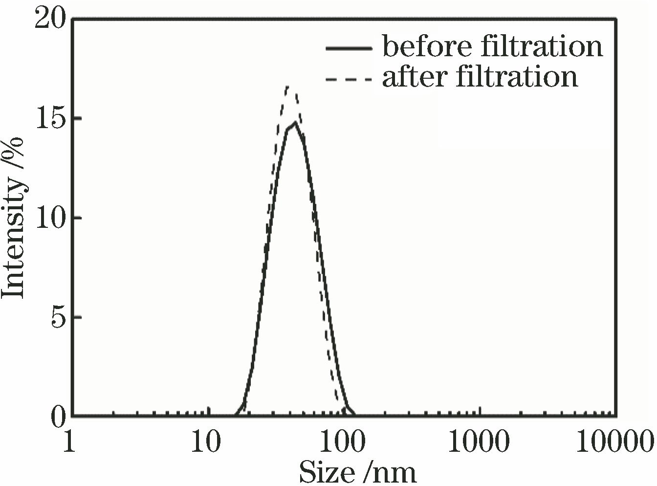
    Fig. 1. Particle distribution of SiO2 coating solutions before and after filtration
    Process flow chart of ultrasonic cleaning
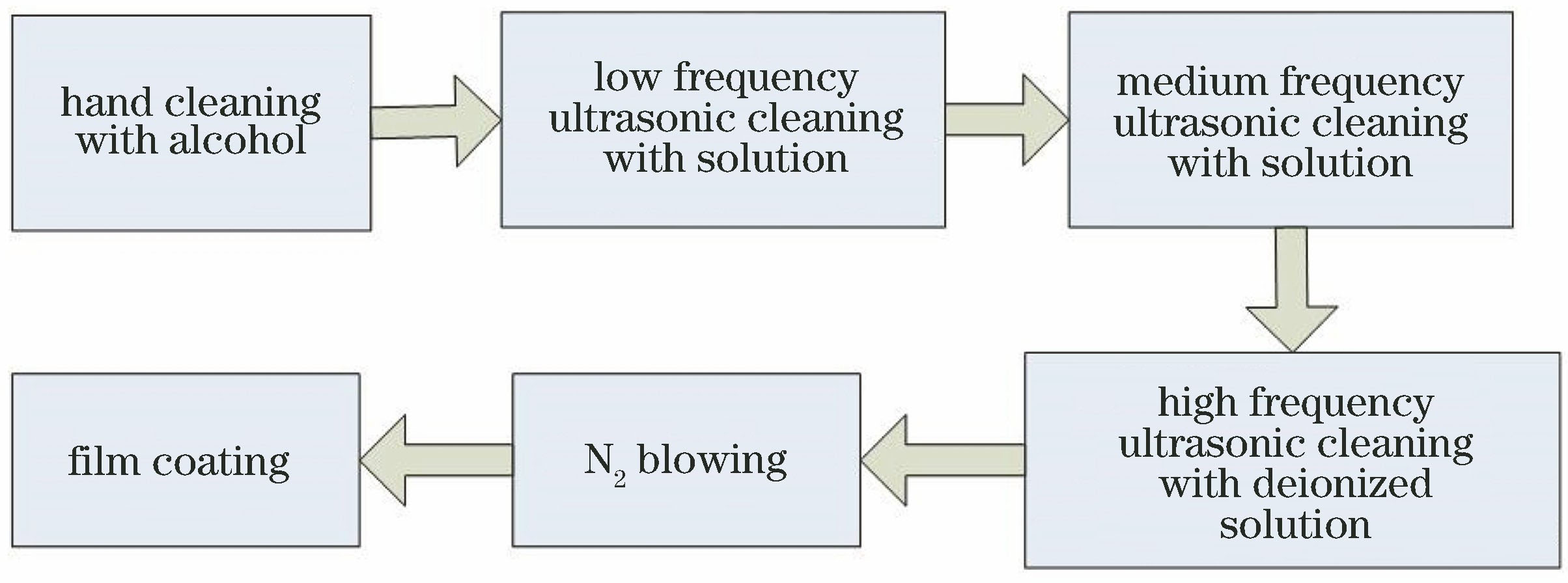
    Fig. 2. Process flow chart of ultrasonic cleaning
    Surface of substrate after hand cleaning. (a) Enlarged by 50 times; (b) enlarged by 200 times
    Fig. 3. Surface of substrate after hand cleaning. (a) Enlarged by 50 times; (b) enlarged by 200 times
    Surface of substrate after ultrasonic cleaning. (a) Enlarged by 50 times; (b) enlarged by 200 times
    Fig. 4. Surface of substrate after ultrasonic cleaning. (a) Enlarged by 50 times; (b) enlarged by 200 times
    Films on small size square KDP crystals by single spin coating method. (a) 3ω; (b) 1ω/2ω
    Fig. 5. Films on small size square KDP crystals by single spin coating method. (a) 3ω; (b) 1ω/2ω
    Transmittance of small size square crystals coated film
    Fig. 6. Transmittance of small size square crystals coated film
    Damage thresholds of films before and after defect control
    Fig. 7. Damage thresholds of films before and after defect control
    Cleaning methodsContact angle 1Contact angle 2Contact angle 3Contact angle 4
    Hand cleaning /(°)62.159.366.163.0
    Ultrasonic cleaning /(°)38.737.937.735.1
    Table 1. Water contact angles of substrates with different cleaning methods
    AreaAfter coating 3ω antireflection filmAfter coating 1ω/2ω antireflection film
    Peak transmittance /%Peak wavelength /nmPeak transmittance /%Peak wavelength /nm
    1>99.6343-355>99.9689-702
    2>99.7338-353>99.8694-702
    3>99.7338-349>99.8709-720
    4>99.5348-359>99.9694-702
    5>99.6347-360>99.9710-720
    Table 2. Transmittance peak wavelengths of small size square crystals coated film
    Bin Shen, Haiyuan Li, Xu Zhang. Properties of Sol-Gel-Modified SiO2 Antireflective Films by Spin Coating[J]. Laser & Optoelectronics Progress, 2019, 56(14): 141602
    Download Citation