• Journal of Semiconductors
  • Vol. 42, Issue 9, 092101 (2021)
Fangxing Zha1, Qiuying Zhang1, Haoguang Dai1, Xiaolei Zhang2、3, Li Yue2, Shumin Wang4, and Jun Shao5
Author Affiliations
  • 1Physics Department, Shanghai University, Shanghai 200444, China
  • 2Shanghai Institute of Microsystem and Information Technology, Chinese Academy of Sciences, Shanghai 200050, China
  • 3School of Information Science and Technology, Shanghai Tech University, Shanghai 201210, China
  • 4Department of Microtechnology and Nanoscience, Chalmers University of Technology, 41296 Gothenburg, Sweden
  • 5National Laboratory for Infrared Physics, Shanghai Institute of Technical Physics, Chinese Academy of Sciences, Shanghai 200083, China
  • show less
    DOI: 10.1088/1674-4926/42/9/092101 Cite this Article
    Fangxing Zha, Qiuying Zhang, Haoguang Dai, Xiaolei Zhang, Li Yue, Shumin Wang, Jun Shao. The scanning tunneling microscopy and spectroscopy of GaSb1–xBix films of a few-nanometer thickness grown by molecular beam epitaxy[J]. Journal of Semiconductors, 2021, 42(9): 092101 Copy Citation Text show less
    (Color online) The STM images and topographic line profiles of (a, b) the GaSb buffer layer, (c, d) the 5 nm GaSbBi layer and (e, f) 10 nm GaSbBi layer, respectively.
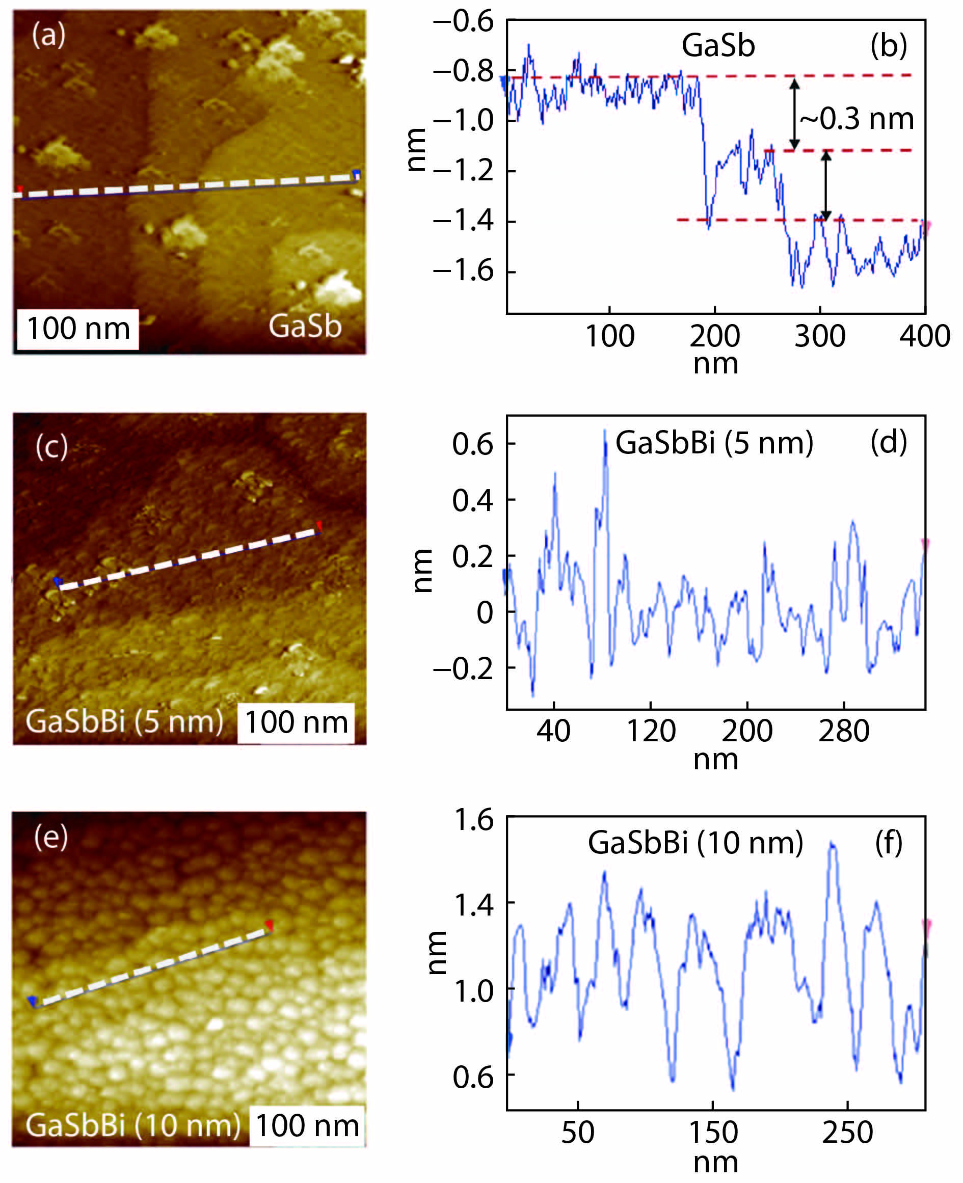
    Fig. 1. (Color online) The STM images and topographic line profiles of (a, b) the GaSb buffer layer, (c, d) the 5 nm GaSbBi layer and (e, f) 10 nm GaSbBi layer, respectively.
    (Color online) (a) The STM image of the GaSb buffer with the indication of the positions of the STS measurements. The arrow designates the position of the I–V curve shown in (b), which is a typical I–V spectrum of GaSb indicating that the current plateau is approximately equal to the band gap of GaSb. (c) The bar graph on the energy distribution of band gaps based on all measured positions in (a).
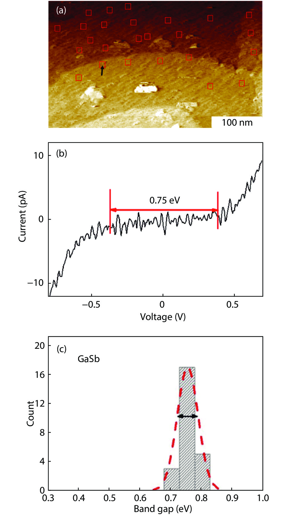
    Fig. 2. (Color online) (a) The STM image of the GaSb buffer with the indication of the positions of the STS measurements. The arrow designates the position of the I–V curve shown in (b), which is a typical I–V spectrum of GaSb indicating that the current plateau is approximately equal to the band gap of GaSb. (c) The bar graph on the energy distribution of band gaps based on all measured positions in (a).
    (Color online) (a) The STM image of the 5 nm GaSb1–xBix layer with the positions of STS measurements marked and the arrows indicate the positions for the I–V curves shown in (b–d). (e) The bar graph on the distribution of energy band gaps measured with respect to the measurement positions in (a).
    Fig. 3. (Color online) (a) The STM image of the 5 nm GaSb1–xBix layer with the positions of STS measurements marked and the arrows indicate the positions for the I–V curves shown in (b–d). (e) The bar graph on the distribution of energy band gaps measured with respect to the measurement positions in (a).
    (Color online) (a) The STM image of the 10 nm GaSb1–xBix film with the positions of STS measurements indicated. (b) The bar graph on the distribution of energy band gaps measured.
    Fig. 4. (Color online) (a) The STM image of the 10 nm GaSb1–xBix film with the positions of STS measurements indicated. (b) The bar graph on the distribution of energy band gaps measured.
    Fangxing Zha, Qiuying Zhang, Haoguang Dai, Xiaolei Zhang, Li Yue, Shumin Wang, Jun Shao. The scanning tunneling microscopy and spectroscopy of GaSb1–xBix films of a few-nanometer thickness grown by molecular beam epitaxy[J]. Journal of Semiconductors, 2021, 42(9): 092101
    Download Citation