
Fangxing Zha, Qiuying Zhang, Haoguang Dai, Xiaolei Zhang, Li Yue, Shumin Wang, Jun Shao. The scanning tunneling microscopy and spectroscopy of GaSb1–xBix films of a few-nanometer thickness grown by molecular beam epitaxy[J]. Journal of Semiconductors, 2021, 42(9): 092101
- Journal of Semiconductors
- Vol. 42, Issue 9, 092101 (2021)
Abstract
1. Introduction
The diluted-bismuth (Bi) semiconductors attract much attention due to their value for near-/mid-infrared (IR) detectors and lasers[
However, the growth of high-quality bismide semiconductors has been a challenge due to the large lattice strain with the incorporation of the Bi atoms. There is still insufficient knowledge on the growth of these largely strained semiconductor films and only a few studies have been concerned with the topic until now[
In order to obtain insight into the growth mechanism of GaSb1–xBix epitaxy, it is meaningful to resort to the thin films with only a few atomic layers grown, whose growth is least interfered by the factors like dislocations, miscibility gaps and segregations, which generally accumulate with the growth thickness. Hence, we were motivated to characterize GaSb1–xBix films of a few nanometers thickness. For the purpose, the samples with two GaSb1–xBix layer thicknesses, i.e. 5 and 10 nm, respectively, were grown and characterized with the ultrahigh vacuum scanning tunneling microscope (UHV STM). The measurement shows that the growth mode of epitaxy may change with the increase of layer thickness: the morphology of the 5 nm film implies the two-dimensional (2D) Frank–van der Merwe (FM) growth mode[
2. Experiment
GaSb1–xBix was grown on Te-doped n-type GaSb substrates using a DCA P600 MBE system, equipped with a valved cracker Sb cell and dual filament effusion cells for Ga and Bi. After the oxide desorption at 660 °C, a 100 nm undoped GaSb buffer layer was grown at 580 °C. Then, the substrate temperature was cooled down to 340 °C to grow the 5 and 10 nm GaSb1–xBix layer, respectively. All the substrate temperature was measured by a thermocouple, which is estimated to be about 100 °C higher than the real temperature. This difference of temperature was calibrated by observing the critical temperature of 370 °C at which the reflection high-energy electron diffraction (RHEED) reconstruction pattern transforms from (1 × 3) to (1 × 5)[
3. Results and discussions
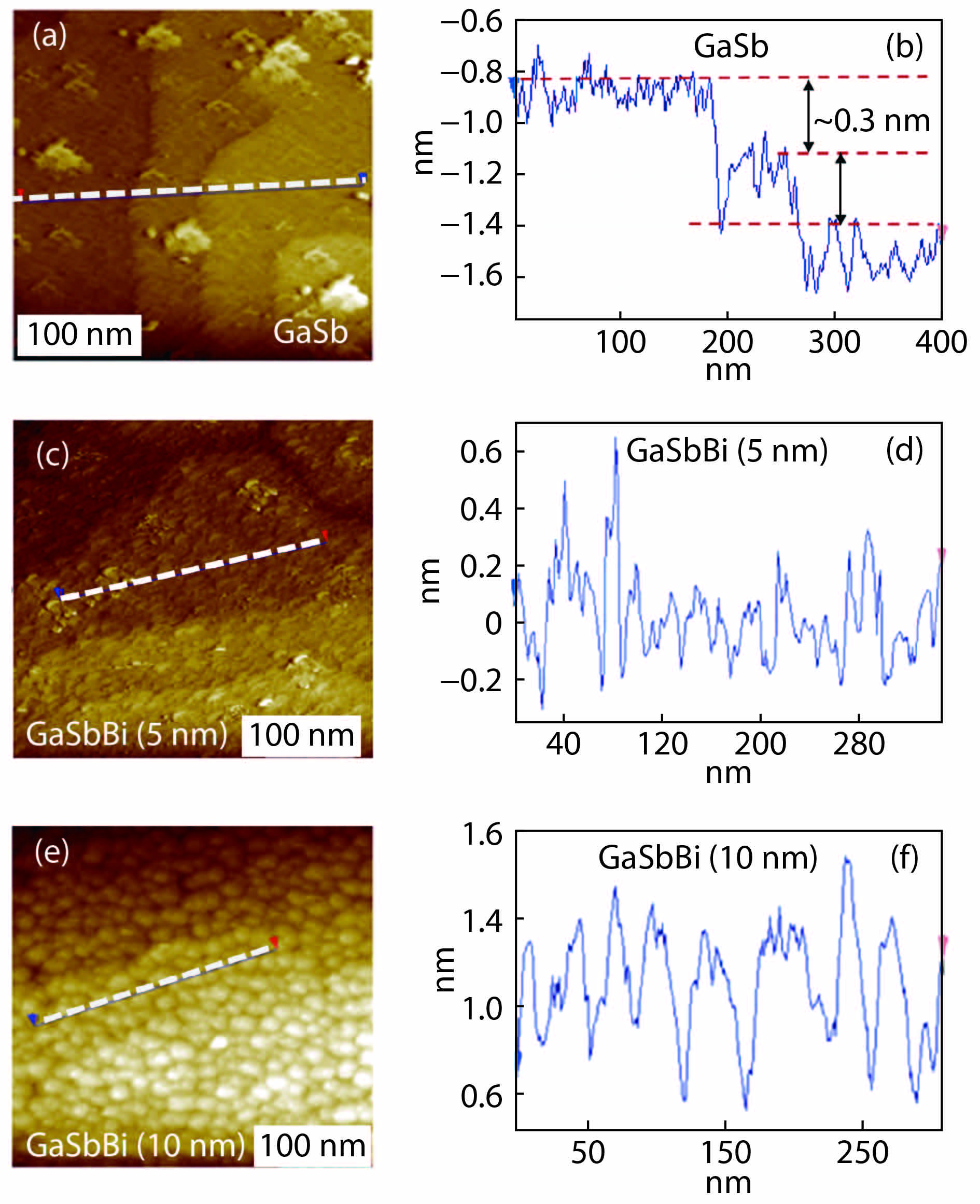
In order to compare with the results on the minor-layer GaSb1–xBix films, the surface of the GaSb buffer layer was also characterized and the STM image is shown in Fig. 1(a). The morphology displays the terraced structure and the topographic line profile shown in Fig. 1(b) indicates that each terrace is atomically flat and the steps of the terraces have the value of ~ 0.3 nm, which is of a one-monolayer (1 ML) thickness of the (100) GaSb faces. The height fluctuation within a terrace is generally smaller than 1 ML, indicating that the growth mode of epitaxy of the 100 nm GaSb buffer layer belongs to the two-dimensional Frank–van der Merwe (FM) mode[
![]()
Figure 1.(Color online) The STM images and topographic line profiles of (a, b) the GaSb buffer layer, (c, d) the 5 nm GaSbBi layer and (e, f) 10 nm GaSbBi layer, respectively.
The result of the 5 nm GaSb1–xBix film is shown in Fig. 1(c). The morphology reserves the same terraced feature as that of the GaSb buffer. The line profile shown in Fig. 1(d) shows that the roughness of the terrace is around ~ 0.4 nm, which is slightly larger than the case of the GaSb surface. This result is interpretable regarding that the lattice constant of GaSb1–xBix is larger than that of GaSb due to the large Bi atoms. Nevertheless, the same terraced feature manifested by 5 nm GaSb1–xBix layer implies that its growth belongs to the same FM mode as that of the GaSb buffer.
In contrast, a distinctive change has been observed for 10 nm GaSb1–xBix film, as shown in Fig. 1(e). The STM image displays the mound-like island morphology. The line profile in Fig. 1(f) reveals that the average height variation is about 0.8 nm, more than 2 MLs thick, indicating that the growth mode is no longer the FM mode but has evolved to the SK mode[
The effect of Bi incorporation in GaSb1–xBix may be evaluated further by the STS measurement since the surface electronic structure is correlated with the Bi composition. An STS spectrum shown herein is acquired in such a way that during the imaging the instrument temporarily suspends tip scanning, moves the STM tip to the desired position, switches off the feedback loop and then conducts a voltage ramp to measure the tunneling current so that an I–V spectrum is produced. For comparing purposes, we first show the STS measurements of the GaSb buffer. A typical I–V spectrum corresponding to the arrow indicated that the position in Fig. 2(a) displays the line-shape with a current plateau at the zero-voltage range. The plateau indicates a gap of 0.75 eV, which is equal to the energy band gap of bulk GaSb at room temperature. We would like to point out that the extraction of the band gap value by the raw I–V data other than by the form of dI/dV or normalized dI/dV is a more accurate assignment herein because the differential of I–V curve is generally noisy and necessarily demands the process of arithmetic data-smoothing, which introduces a larger uncertainty of the assignment. To be more convincible with the extraction of band gap value, a variety of measurements, with the arbitrarily selected positions as the indication of the square labels in Fig. 2(a), were performed. One may obtain a statistical view with the bar graph plot as shown in Fig. 2(c). From the total of twenty-six measurements, the bar graph exhibits the count number for the different energy ranges, which are in an interval of 0.05 eV. The dashed-line curve with the bar graph is the Gaussian distribution calculated with the average plateau width and the corresponding root of mean square (RMS) value, which are 0.757 and 0.034 eV, respectively. The RMS, reflecting the uncertainty of the measurement, is about 4.5% of the mean value and equal to the half-width of the horizontal arrow line designated in Fig. 2(c).
![]()
Figure 2.(Color online) (a) The STM image of the GaSb buffer with the indication of the positions of the STS measurements. The arrow designates the position of the
Note that the average value of 0.757 eV is approximately equal to the energy band gap of bulk GaSb at 300 K, validating the assignment of the flat band model. Nevertheless, some current plateaus displaying larger values than the intrinsic energy band gap indicates that the tip-induced band bending effect is not negligible with some measurement locations[
In the following, we apply the above analysis on the STS results of the GaSb1–xBix films. Fig. 3(a) is the STM image of the 5 nm GaSb1–xBix film, in which the locations of STS measurements are marked with the squares. The measured band gaps with the positions marked in (a) are distributed in a wider energy range of 0.4–0.7 eV. Figs. 3(b)–2(d) display three representative I–V curves, which correspond to the arrow-indicated positions with the numbers 1–3 in Fig. 3(a). The mean band gap value calculated with all spectra, is found to be 0.571 eV and the RMS value is 0.059 eV. Note that the RMS herein is about 10% of the mean band gap value, more dispersed than the case of GaSb. Such an effect should arise from the spatial inhomogeneity of the Bi atoms. According to the relationship of the energy band gap and Bi composition x[
![]()
Figure 3.(Color online) (a) The STM image of the 5 nm GaSb1–
In contrast, the analysis of the 10 nm GaSb1–xBix generates a different result. Fig. 4(a) is an STM image of 10 nm film marked with the positions of the STS measurements. The corresponding bar graph resulting from twenty pieces of data is shown in Fig. 4(b). For this sample, the mean energy band gap is found to be 0.531 eV, which is smaller than the result of 5 nm. It corresponds the Bi composition of x = 0.071, larger than that of the 5 nm GaSb1–xBix film which shows x = 0.058. The result implies the increase of Bi incorporation with the layer growth. On the other hand, the RMS value increases to 0.079 eV, which is about 15% of the mean band gap value. Accordingly, the x value is generally in the range of (0.045, 0.097). It means that the spatial inhomogeneity of Bi has also turned to a larger range in the 10 nm GaSb1–xBix film case. The comparison with the calculated Gaussian distributions between Fig. 4(b) and Fig. 3(b) provides an intuitive demonstration on the point.
![]()
Figure 4.(Color online) (a) The STM image of the 10 nm GaSb1–
4. Conclusion
In conclusion, the present study preforms the STM & STS characterization on the GaSb 1–xBix films of a few nanometers thickness. The study shows that the growth is initially attributed to the FM growth mode as revealed by the morphology of 5 nm GaSb1–xBix film but is transformed to the SK growth mode subsequently as indicated by that of the 10 nm film. The analysis of the position-dependent STS measurements provides insight into the spatial distribution of Bi composition. The comparison on the 5 and 10 nm films discloses the growth mechanism on the initial epitaxial stage of GaSb1–xBix, indicating that the composition as well as the spatial inhomogeneity of Bi atoms increases with the growth thickness.
Acknowledgements
This work was supported by the National Natural Science Foundation of China (Nos. 61474073, 61874069 and 61804157).
References
[1]
[2] E Luna, O Delorme, L Cerutti et al. Microstructure and interface analysis of emerging Ga(Sb, Bi) epilayers and Ga(Sb, Bi)/GaSb quantum wells for optoelectronic applications. Appl Phys Lett, 112, 151905(2018).
[3] S Souto, J Hilska, Gobato Y Galvão et al. Raman spectroscopy of GaSb1−
[4] C B Pan, F X Zha, Y X Song et al. Spectral and spatial resolving of photoelectric property of femtosecond laser drilled holes of GaSb1−
[5] O Delorme, L Cerutti, E Luna et al. GaSbBi/GaSb quantum well laser diodes. Appl Phys Lett, 110, 222106(2017).
[6] K Alberi, J Wu, W Walukiewicz et al. Valence-band anticrossing in mismatched III-V semiconductor alloys. Phys Rev B, 75, 045203(2007).
[7] S Francoeur, M J Seong, A Mascarenhas et al. Band gap of GaAs1−
[8] M K Rajpalke, W M Linhart, K M Yu et al. Bi-induced band gap reduction in epitaxial InSbBi alloys. Appl Phys Lett, 105, 212101(2014).
[9] A J Shalindar, P T Webster, B J Wilkens et al. Measurement of InAsBi mole fraction and InBi lattice constant using Rutherford backscattering spectrometry and X-ray diffraction. J Appl Phys, 120, 145704(2016).
[10] S M Wang, I Saha Roy, P X Shi et al. Growth of GaSb1–
[11] O Delorme, L Cerutti, E Luna et al. Molecular-beam epitaxy of GaInSbBi alloys. J Appl Phys, 126, 155304(2019).
[12] L J Wang, L Y Zhang, L Yue et al. Novel dilute bismide, epitaxy, physical properties and device application. Crystals, 7, 63(2017).
[13] M K Rajpalke, W M Linhart, M Birkett et al. High Bi content GaSbBi alloys. J Appl Phys, 116, 043511(2014).
[14] L Yue, X Chen, Y C Zhang et al. Structural and optical properties of GaSbBi/GaSb quantum wells. Opt Mater Express, 8, 893(2018).
[15] A Duzik, J M Millunchick. Surface morphology and Bi incorporation in GaSbBi(As)/GaSb films. J Cryst Growth, 390, 5(2014).
[16] L Yue, X Chen, Y Zhang et al. Molecular beam epitaxy growth and optical properties of high bismuth content GaSb1–
[17] E Bauer, J H van der Merwe. Structure and growth of crystalline superlattices: From monolayer to superlattice. Phys Rev B, 33, 3657(1986).
[18] K Yamaguchi, K Yujobo, T Kaizu. Stranski-Krastanov growth of InAs quantum dots with narrow size distribution. Jpn J Appl Phys, 39, L1245(2000).
[19] P M Thibado, B R Bennett, B V Shanabrook et al. A RHEED and STM study of Sb-rich AlSb and GaSb (001) surface reconstructions. J Cryst Growth, 175/176, 317(1997).
[20] F X Zha, F Hong, B C Pan et al. Atomic resolution on the (111)B surface of mercury cadmium telluride by scanning tunneling microscopy. Phys Rev B, 97, 035401(2018).
[21] R M Feenstra. Tunneling spectroscopy of the (110) surface of direct-gap III–V semiconductors. Phys Rev B, 50, 4561(1994).
[22] F X Zha, M S Li, J Shao et al. Implication of exotic topography depths of surface nanopits in scanning tunneling microscopy of HgCdTe. Appl Phys Lett, 101, 141604(2012).
[23] M P Polak, P Scharoch, R Kudrawiec. First-principles calculations of bismuth induced changes in the band structure of dilute Ga–V–Bi and In–V–Bi alloys: Chemical trends versus experimental data. Semicond Sci Technol, 30, 094001(2015).

Set citation alerts for the article
Please enter your email address
© Copyright 2018-2021 | Chinese Laser Press. All Rights Reserved 沪ICP备15018463号-20