
Jie Zhang, Shixin Hou, Renjie Li, Bingbing Chen, Fuhua Hou, Xinghua Cui, Jingjing Liu, Qi Wang, Pengyang Wang, Dekun Zhang, Ying Zhao, Xiaodan Zhang. I/P interface modification for stable and efficient perovskite solar cells[J]. Journal of Semiconductors, 2020, 41(5): 052202
- Journal of Semiconductors
- Vol. 41, Issue 5, 052202 (2020)
Abstract
1. Introduction
Organic–inorganic halide perovskite solar cells (PSCs) have been rapid developed in the past decade due to their unique properties, such as high carrier mobility, low-cost fabrication, adjustable band-gap, simple solution-based processes, and long carrier diffusion length, etc.[
Interface passivation is increasingly essential for enhancing the performance of PSCs. For example, You et al. reported that excess PbI2 on the surface or grain boundaries of perovskite films can suppress charge recombination[
In this work, in order to reduce the interface iodide deficiency for FA-based PSCs, we adopted an interface passivation method by using MABr reacted with excess PbI2 to form a perovskite passivation layer between the hole transport layer (HTL) and perovskite absorber interface. The result demonstrates a decrease in surface defects and non-radiative recombination, and an increase in carrier extraction. So that, we obtain an enhanced PCE of 20.83%, which is superior to the control device with a PCE of 18.39%. In addition, the device indicates outstanding stability of humidity and temperature.
2. Experimental section
2.1. Materials
Isopropyl alcohol (IPA), N,N-dimethylformamide (DMF) and dimethylsulfoxide (DMSO) were obtained from Sigma Aldrich. SnO2 precursor was purchased from Alfa Aesar. Other materials were obtained from Xi’an Polymer Light Technology Corp.
2.2. Film and device fabrication
First, the ITO glass substrates were immersed in industrial cleaning agents, acetone and isopropyl alcohol, for 40 min each for ultrasonic cleaning. Then they were put on the ultraviolet ozone machine platform and removed after 20 min of ozone treatment. The prepared tin dioxide solution (15% strength tin dioxide solution : ammonia = 1 : 3) was dropped on the ITO, which was spin-coated at a speed of 4000 rpm for 30 s, and then placed on a heating plate at 150 °C for 30 min. Ozone treatment was used for another 20 min. Dropped the configured FAMACs perovskite precursor solution containing FAI (1.1 M), PbI2 (1.2 M), MABr (0.05 M), CsI (0.10 M), MACl (0.05 M) in mixture DMF : DMSO = 2 : 3 (v/v) on the tin dioxide layer, spin-coated at 1000 rpm for 10 s, then at 5000 rpm for 50 s during which in the last 20 s 100 µL of anti-solvent chlorobenzene was added. Put it directly on a 130 °C heating plate for 30 min. For the surface passivation treatment, cooled down the films to room temperature and dropped 60 µL of 2 mg/mL isopropyl alcohol solution containing MABr on the surface of the perovskite layer, and spin-coated it at a speed of 4000 rpm for 30 s, then placed it on a 90 °C heating plate for 5 min. Next, dropped 35 µL Spiro-OMeTAD on the surface of the passivation layer or perovskite layer, and then spin-coated at a speed of 4000 rpm for 30 s. At last, a layer of 80-nm gold top electrode was deposited by thermal evaporation.
2.3. Film and device characterization
The XRD patterns were obtained by Rigaku MiniFlex 600 using Kα radiation (λ = 1.5406 Å) to measure the crystal structure. In order to obtain the surface structure of the perovskite film, the SEM image was tested by FEI NanoSEM650. For getting the information of carrier lifetime, PL and TRPL tests were performed by fluorescence spectrophotometer (Edinburgh FS5). Current density–voltage (J–V) characteristics were obtained at the room temperature under AM 1.5G illumination by Keithley 2400 through a mask with an area of 0.089 cm2. The dark density–voltage (J–V) characteristics were obtained under dark condition by Keithley 2400. The surface morphology of perovskite film was obtained by NanoNavi-SPA400. The EQE spectra in ambient air were obtained by QEX10 instrument at room temperature.
3. Results and discussion
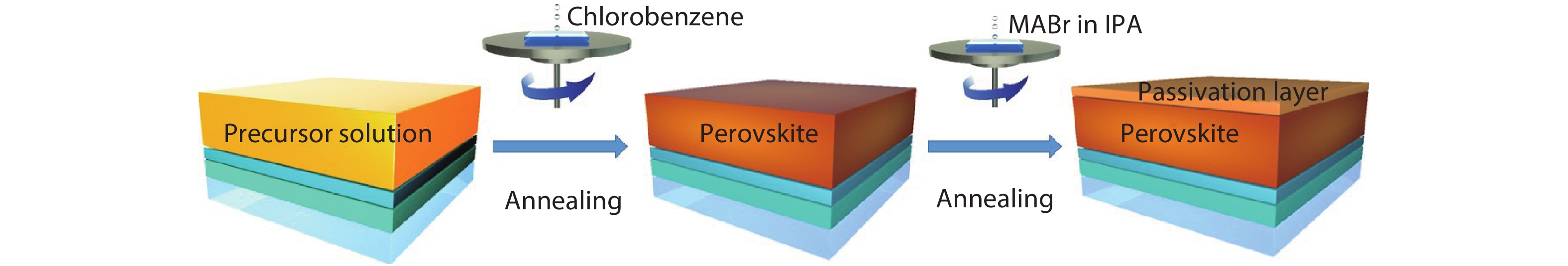
The formation process of perovskite passivation film is shown in Fig. 1. Proper amount of PbI2 in grain boundaries could passivate the defects and deliver higher efficiency[
![]()
Figure 1.(Color online) Schematic diagram of the formation of passivation layer.
The scanning electron microscopy (SEM) images of perovskite films with and without modification are shown in Figs. 2(a) and 2(b), respectively. It can be deduced that the surface of perovskite film with modification is flatter. From the atom force microscopy (AFM) measurement shown in Figs. 2(c) and 2(d), it can be regarded that the passivation layer results in smoother perovskite films. Root mean square (RMS) of the passivated and control films are 17.04 and 17.89 nm, respectively. Fig. 2(e) shows the device structure diagram of the passivated perovskite solar cells. The results of X-ray diffraction (XRD) are shown in Fig. 2(f). The diffraction peak of PbI2 (12.6°) decreases sharply after spin-coating of the MABr, which indicats that a new perovskite is formed due to the reaction of excessive PbI2 with MABr[
![]()
Figure 2.(Color online) SEM and AFM images of (a, c) control and (b, d) passivated perovskite films on ITO/SnO2 substrates. (e) Device structure of the passivated perovskite solar cells. (f) XRD patterns of passivated and control perovskite films.
Fig. 3(a) shows the I–V relationship of the devices with and without I/P interface passivation. The efficiency increased from 18.39% to 19.97%. Current density did not change greatly, but the Voc and the FF increased from 1.10 to 1.14 eV and from 73.98% to 77.03%, respectively. Fig. 3(b) shows the external quantum efficiency (EQE) spectra of the passivated and original devices. It can be found that the integrated current densities of control and passivated perovskite solar cell are 22.03 and 21.80 mA/cm2, respectively, which shows the same trend with the J–V results.
![]()
Figure 3.(Color online) (a)
Ultraviolet photoelectron spectroscopy (UPS) measurements of glass/ITO/perovskite and glass/ITO/perovskite/passivation substrates were used to further study the energy band structure[
![]()
Figure 4.(Color online) (a) Spectra of ultraviolet photoelectron spectroscopy (UPS). (b) Secondary electron cutoff and (c) valence band region near EF of the perovskite film without (control) and with MABr (2 mg/mL) deposited on ITO substrate. (d) The energy level diagram of PSCs. (e) Steady-state photoluminescence (PL) and (f) time-resolved PL (TRPL) spectra of the passivated and control perovskite film.
Here, τ1 and τ2 are the fast and slow recombination lifetimes, and A1 and A2 are the relative amplitudes. The τ1 value of the ITO/perovskite/passivation layer/spiro is smaller than that of the ITO/perovskite/spiro, which indicates that the interface has fewer defects. The detailed results are shown in Table 2. This conclusion is also consistent with UPS and PL, and shows the ultimately improvement of the electrical performance of PSCs.
In order to better evaluate the trap density of both perovskite films, space-charge-limited current (SCLC) was conducted under dark conditions with the glass/ITO/perovskite/Au (Figs. 5(a) and 5(b)) device structure. The calculation formula of ntrap can be described by[
![]()
Figure 5.(Color online)
where VTFL is the trap-filled limit (TFL) voltage, e is the electric charge, d is the thickness of the perovskite layer, ε0 is the vacuum permittivity, and ε is the dielectric constant of the perovskite layer. The calculated trap state densities are 1.51 × 10¹⁶ and 1.38 × 1016 cm–3 for the control and passivated perovskite, respectively[
Eighty samples with or without passivation layer were prepared in different batches, and the average values of PCE are shown in Fig. 6(a), respectively. The average PCE of controlled sample is about 18.40%, while passivated devices is about 20.00%. Fig. 6(b) presents the J−V curves with forward and reverse scanning directions of champion device with passivated perovskite solar cell. The best-performing device achieves a PCE of 20.83% from forward scan with a Voc of 1.14 V, Jsc of 23.28 mA/cm2 and FF of 78.83%. Fig. 6(c) shows the EQE curve of PSCs, as we can calculate that the integrated Jsc value is 22.34 mA/cm2. In addition, the current density is measured at a fixed maximum voltage (0.97 V) and a steady power output (SPO) for 300 s, as shown in Fig. 6(d).
![]()
Figure 6.(Color online) (a) Histogram distribution of the PCE for devices with control (40 cells) and passivated perovskite films (40 cells). (b)
The performance of passivated PSCs was also evaluated from the perspective of device stability, humidity and thermal stability of the device were carried out. Fig. 7(a) is the stability of devices under humidity (20%–30%) without encapsulation. After 1000 hours, the passivated device could maintain 94% of its initial efficiency (from 19.62% to 18.48%). In contrast, the control device only maintains 70% of its initial efficiency (from 18.30% to 12.91%). We also examine the thermal stability of both devices under ambient air with encapsulation (65 °C), as shown in Fig. 7(b). After 400 hours, the passivated device maintains 90% of its initial efficiency, which means that the passivated devices have better stability under continuous heating at 65 °C.
![]()
Figure 7.(Color online) (a) PCEs evolution of devices in ambient air with the room temperature of 25–30 °C, and the humidity of 20%–30%. (b) Devices kept at 65 °C in ambient air with encapsulation for 400 h.
We also performed XRD test for control and passivated perovskite films in humidity stability test. As we can see in Fig. 8, the yellow phase perovskite peaks appear earlier in the control group, which indirectly reflects that the passivation layer could effectively prevent the water in ambient air from contacting the perovskite absorption layer, thus reduce the influence of water on the perovskite and promote the water stability of the PSCs.
![]()
Figure 8.(Color online) XRD patterns of (a) control and (b) passivated perovskite films after in humid air (with RH: 20%−30%) for 0, 100, 400, 700, and 1000 h.
Stability is the most important key characteristic for perovskite solar cells. This research shows that the device stability after passivation has been improved. There are two possible reasons. First of all, excessive PbI2 is detrimental to device stability[
4. Conclusion
To promote the electrical properties of PSCs, we introduced a passivation layer between hole transport and perovskite absorber layer. Through the UPS measurement, we found that the energy level after passivation is more matched. The SCLC and TRPL results show that the passivation layer can effectively reduce surface defects and non-radiative recombination, while increase carrier extraction. Ultimately, we obtained a champion device with efficiency of 20.83%. This method also provides enhanced humidity and thermal stability. As a result, the device retains about 94% of its initial PCE after 1000 h under ambient air without encapsulation. We believe that the surface modification strategy will help researchers to achieve efficient and stable PSCs.
Acknowledgements
The authors gratefully acknowledge the supports from National Key Research and Development Program of China (Grant No. 2018YFB1500103), the National Natural Science Foundation of China (Grant No. 61674084), the Overseas Expertise Introduction Project for Discipline Innovation of Higher Education of China (Grant No. B16027), Tianjin Science and Technology Project (Grant No. 18ZXJMTG00220), and the Fundamental Research Funds for the Central Universities, Nankai University (Grant Nos. 63191736, ZB19500204).
References
[1] W S Yang, J H Noh, N J Jeon et al. High-performance photovoltaic perovskite layers fabricated through intramolecular exchange. Science, 348, 1234(2015).
[2] Q Dong, Y Fang, Y Shao et al. Electron-hole diffusion lengths > 175
[3] M I Saidaminov, A L Abdelhady, B Murali et al. High-quality bulk hybrid perovskite single crystals within minutes by inverse temperature crystallization. Nat Commun, 6, 1(2015).
[4] Q Han, S H Bae, P Sun et al. Single crystal formamidinium lead iodide (FAPbI3): insight into the structural, optical, and electrical properties. Adv Mater, 28, 2253(2016).
[5] S Chu, Y Cui, N Liu. The path towards sustainable energy. Nat Mater, 16, 16(2017).
[6] D P McMeekin, G Sadoughi, W Rehman et al. A mixed-cation lead mixed-halide perovskite absorber for tandem solar cells. Science, 351, 151(2016).
[7] A Kojima, K Teshima, Y Shirai et al. Organometal halide perovskites as visible-light sensitizers for photovoltaic cells. J Am Chem Soc, 131, 6050(2009).
[8] H S Kim, C R Lee, J H Im et al. Lead iodide perovskite sensitized all-solid-state submicron thin film mesoscopic solar cell with efficiency exceeding 9%. Sci Rep, 2, 591(2012).
[9] Q Jiang, Y Zhao, X Zhang et al. Surface passivation of perovskite film for efficient solar cells. Nat Photonics, 13, 460(2019).
[10]
[11] F C Hanusch, E Wiesenmayer, E Mankel et al. Efficient planar heterojunction perovskite solar cells based on formamidinium lead bromide. J Phys Chem Lett, 5, 2791(2014).
[12]
[13] T Xu, L Chen, Z Guo et al. Strategic improvement of the long-term stability of perovskite materials and perovskite solar cells. Phys Chem Chem Phys, 18, 27026(2016).
[14] X Zheng, B Chen, J Dai et al. Defect passivation in hybrid perovskite solar cells using quaternary ammonium halide anions and cations. Nat Energy, 2, 17102(2014).
[15] W S Yang, B W Park, E H Jung et al. Iodide management in formamidinium-lead-halide–based perovskite layers for efficient solar cells. Science, 356, 1376(2017).
[16] F Wang, S Bai, W Tress et al. Defects engineering for high-performance perovskite solar cells. npj Flexible Electron, 2, 1(2018).
[17] L Meng, C Sun, R Wang et al. Tailored phase conversion under conjugated polymer enables thermally stable perovskite solar cells with efficiency exceeding 21%. J Am Chem Soc, 140, 17255(2018).
[18] Y Bai, X Meng, S Yang. Interface engineering for highly efficient and stable planar p–i–n perovskite solar cells. Adv Energy Mater, 8, 1701883(2018).
[19] T S Sherkar, C Momblona, L Gil-Escrig et al. Recombination in perovskite solar cells: significance of grain boundaries, interface traps, and defect ions. ACS Energy Lett, 2, 1214(2017).
[20] M Moriya, D Hirotani, T Ohta et al. Architecture of the interface between the perovskite and hole-transport layers in perovskite solar cells. ChemSusChem, 9, 2634(2016).
[21] H Tan, F Che, M Wei et al. Dipolar cations confer defect tolerance in wide-bandgap metal halide perovskites. Nat Commun, 9, 1(2018).
[22] N Li, S Tao, Y Chen et al. Cation and anion immobilization through chemical bonding enhancement with fluorides for stable halide perovskite solar cells. Nat Energy, 4, 408(2019).
[23] P Wang, R Li, B Chen et al. Gradient energy alignment engineering for planar perovskite solar cells with efficiency over 23%. Adv Mater, 1905766(2020326).
[24] Q Jiang, Z Chu, P Wang et al. Planar-structure perovskite solar cells with efficiency beyond 21%. Adv Mater, 29, 1703852(2017).
[25] S H Turren-Cruz, A Hagfeldt, M Saliba. Methylammonium-free, high-performance, and stable perovskite solar cells on a planar architecture. Science, 362, 449(2018).
[26] Y Wang, T Wu, J Barbaud et al. Stabilizing heterostructures of soft perovskite semiconductors. Science, 365, 687(2019).
[27] P Wang, Q Jiang, Y Zhao et al. Synergistic improvement of perovskite film quality for efficient solar cells via multiple chloride salt additives. Sci Bull, 63, 726(2018).
[28] G Tumen-Ulzii, C Qin, D Klotz et al. Detrimental effect of unreacted PbI2 on the long-term stability of perovskite solar cells. Adv Mater, 1905035(20203216).
[29] J Y Jeng, K C Chen, T Y Chiang et al. Nickel oxide electrode interlayer in CH3NH3PbI3 perovskite/PCBM planar-heterojunction hybrid solar cells. Adv Mater, 26, 4107(2014).
[30] J You, L Meng, T B Song et al. Improved air stability of perovskite solar cells via solution-processed metal oxide transport layers. Nat Nanotechnol, 11, 75(2016).
[31] G Xu, P Bi, S Wang et al. Integrating ultrathin bulk-heterojunction organic semiconductor intermediary for high-performance low-bandgap perovskite solar cells with low energy loss. Adv Funct Mater, 28, 1804427(2018).
[32] J Zhang, R Xue, G Xu et al. Self-doping fullerene electrolyte-based electron transport layer for all-room-temperature-processed high-performance flexible polymer solar cells. Adv Funct Mater, 28, 1705847(2018).
[33] S Wang, T Sakurai, W Wen et al. Energy level alignment at interfaces in metal halide perovskite solar cells. Adv Mater Interfaces, 5, 1800260(2018).
[34] X Li, D Bi, C Yi et al. A vacuum flash-assisted solution process for high-efficiency large-area perovskite solar cells. Science, 353, 58(2016).
[35] N K Noel, A Abate, S D Stranks et al. Enhanced photoluminescence and solar cell performance via Lewis base passivation of organic–inorganic lead halide perovskites. ACS Nano, 8, 9815(2014).
[36] Y Du, C Xin, W Huang et al. Polymeric surface modification of NiO
[37] M A Lampert. Simplified theory of space-charge-limited currents in an insulator with traps. Phys Rev, 103, 1648(1956).
[38] A A Zhumekenov, M I Saidaminov, M A Haque et al. Formamidinium lead halide perovskite crystals with unprecedented long carrier dynamics and diffusion length. ACS Energy Lett, 1, 32(2016).
[39] M Zhang, Q Chen, R Xue et al. Reconfiguration of interfacial energy band structure for high-performance inverted structure perovskite solar cells. Nat Commun, 10, 1(2019).
[40] S Wang, H Chen, J Zhang et al. Targeted therapy for interfacial engineering toward stable and efficient perovskite solar cells. Adv Mater, 31, 1903691(2019).

Set citation alerts for the article
Please enter your email address
© Copyright 2018-2021 | Chinese Laser Press. All Rights Reserved 沪ICP备15018463号-20