
Jialin Sun, Chuncai Hou, Hongmei Chen, Jinchuan Zhang, Ning Zhuo, Jiqiang Ning, Changcheng Zheng, Zhanguo Wang, Fengqi Liu, Ziyang Zhang. Quantum cascade superluminescent light emitters with high power and compact structure[J]. Journal of Semiconductors, 2020, 41(1): 012301
- Journal of Semiconductors
- Vol. 41, Issue 1, 012301 (2020)
Abstract
1. Introduction
Quantum cascade (QC) superluminescent light emitters (SLEs), different from traditional bipolar semiconductor emitters, are unipolar semiconductor broadband edge-emitting light sources based on intersubband transition of electrons in the conduction band[
SLEs based on QC material are the ideal broadband light sources for the MIR-OCT systems[
In this paper, a strain-compensated QC material based on a four-quantum well (QW) coupling and two-phonon resonance structure was utilized to improve the efficiency of amplified spontaneous emission in the intersubband transitions. Based on this QC active region, a combinatorial waveguide structure was demonstrated with a short straight waveguide (SW) adjacent to a tilted waveguide (TW) and to a J-shaped waveguide (JW). This structure would produce two structural mutations to realize a rather low reflectivity with a fairly small geometry and enable the fabrication of long device on a relatively small chip area. Benefiting from these material and device structural designs, the fabricated SLEs have inhibited lasing and achieved a high superluminescent power of 1.8 mW at 80 K in quasi-continuous wave (quasi-CW) mode with a duty circle of 3%. Furthermore, these attempts would facilitate the integration of SLE arrays to attain larger output power and practical applications as broadband MIR light sources in the next step.
2. Experiments
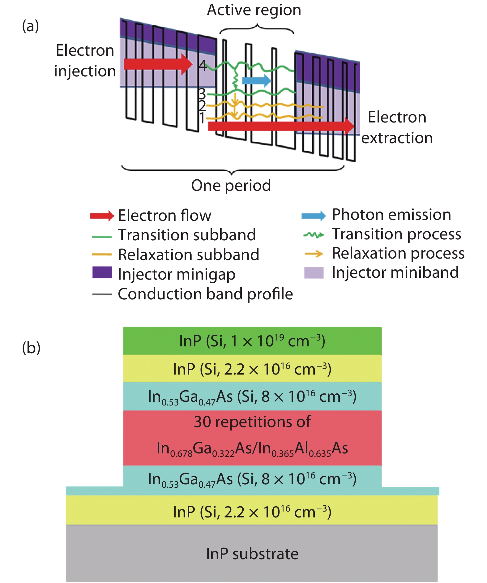
The active region of QC SLEs was grown by solid source molecular beam epitaxy (MBE) in a single growth step on an InP substrate, which consists of the strain-compensated four-QW coupling of In0.678Ga0.322As/In0.365Al0.635As and two-phonon resonance structure. The two-phonon resonance leads to a more efficient electron extraction due to the twice electron pumping by optical phonon scattering. As a result, this structure substantially benefits the population inversion and then enhances the radiative transition rate. Thirty repetitions of the active region/injector are sandwiched by low doped (n ≈ 8 × 1016 cm−3) In0.53Ga0.47As layers. Beginning from the injection barrier, the layer sequence of one period is as follows (thickness in nanometers):
![]()
Figure 1.(Color online) Illustration of (a) the band structure of the four-QW coupling and two-phonon resonance-based QC structure, and (b) the corresponding layered cross-sectional structure of the QC material.
After the MBE growth, the wafer was processed into a 10 μm double-trench narrow ridge waveguide structure by photolithography and wet chemical etching. The waveguide was etched deeply down to 7 μm through the active region to avoid the pronounced current spreading caused by the strong discontinuities of the anisotropic electrical conductivity in the multi-quantum well active region. Fig. 2(a) exhibits the schematic diagram of the double-trench narrow ridge waveguide structure, which is capable of creating a sufficient low reflectivity by the three-section design: a 0.5-mm-long SW adjacent to a 1-mm-long TW and to a 12°-bent 2-mm-long JW. Fig. 2(b) shows the corresponding scanning electron microscope image of the straight end, and Figs. 2(c) and 2(d) present the top-view microscope images of SLE devices with 8°- or 12°-inclined TW, respectively. These images have indicated the high quality of the device fabrication without any observable defect or irregularity. Then, an insulation layer of SiO2 was deposited using plasma-enhanced chemical vapor deposition. The 3-μm-wide contact windows were fabricated on top of the ridges by the techniques of photolithography and reactive ion etching, and the Ti/Au (50/500 nm in thickness) top metal contact was deposited by magnetron sputtering. Afterwards, the wafer was thinned and burnished to about 110 μm, and the Ge/Au/Ni/Au (30/50/15/200 nm in thickness) bottom metal contact was evaporated on the burnished reverse side by electron beam evaporation. Finally, the samples were mounted epitaxial-side down on copper heat sinks to relieve the self-heating effect.
![]()
Figure 2.(Color online) (a) Schematic diagram of the double-trench narrow ridge waveguide structure of SLE devices. (b) Corresponding scanning electron microscope image of the straight end. The top-view microscope images of SLE devices with (c) 8°- or (d) 12°-inclined TW.
3. Results and discussion
The superluminescent light is generated from spontaneous emission and amplified by stimulated emission below the lasing threshold, which is similar to the design of lasers but with the suppression of light oscillations in resonators. It is well known that a tilted or bent waveguide design with relatively small angles cannot offer low reflectivity of < 10 −6 to inhibit lasing in the MIR QC SLEs[
As the inclined angle of TW is the critical factor to acquire such a reflectivity, optical field simulations were performed to find an appropriate inclined angle (denoted as α). The schematic drawings of different waveguide structures with α = 0°, 8° or 12° (on the left) and the corresponding simulated mode distribution results (on the right) are shown in Figs. 3(a)–3(c), respectively. The waveguide with α = 0° is equivalent of a single JW with bent angle of 12°, which is obviously not able to suppress lasing[
![]()
Figure 3.(Color online) Schematic drawings (left) and optical field simulations (right) of the SLEs with (a)
The emission characteristics of the fabricated SLEs were measured from the bent end (front facet, the left end in Fig. 3), which has smaller reflectivity than the straight end (rear facet). The light–current (L–I) curves were collected by a calibrated thermopile detector placed directly in front of the cryostat, and the emission spectra were measured by a Fourier transform infrared spectrometer. As seen in Fig. 4(a), the SLEs with α = 8° exhibit lasing characteristics rather than superluminescence at 80 K in quasi-CW (15 kHz, 2 μs) regime, and the pulsed threshold current is found to be about 780 mA. In Fig. 4(a), the “×” marks the lasing threshold, which is determined from the corresponding spectrum shown in the inset. This experimental observation illustrates that the waveguide structure of such an SLE with α = 8° could not provide a sufficient low reflectivity to suppress lasing and generate superluminescent light, which conforms to the simulation results.
![]()
Figure 4.(Color online) Emission characteristics of SLEs measured under quasi-CW (15 kHz, 2
Then, the SLEs with α = 8° were improved by introducing an Al2O3/Ge (450/35 nm in thickness) AR coating on the rear facet to further suppress lasing. The L–I curve and emission spectra of such an SLE are shown in Figs. 4(b) and 4(c), which were measured at 80 K in the quasi-CW (15 kHz, 2 μs) mode. Lasing was completely suppressed by the AR coating, and superluminescent light emission was observed from the front facet. The output power increases super linearly as a function of injected current, and the maximum superluminescent power is 0.6 mW at 2.6 A. The spectral curves exhibit smooth Gaussian shape, and the full width at half maximum (FWHM) is 36 cm−1 when the optical gain has saturated. The fairly narrowband superluminescent output of the coated SLE indicates that the AR coating can only reluctantly inhibit lasing in this structure. Meanwhile, the output power is also relatively low due to the substantial optical loss caused by the AR coating. Therefore, the waveguide structure with α = 8° is not suitable for fabricating high-power and broadband MIR SLEs.
To obtain more desirable MIR SLEs, the SLEs with α = 12° were fabricated according to the simulation results. Fig. 5 exhibits the emission characteristics of such a SLE at 80 K in quasi-CW (15 kHz, 2 μs) mode. As seen from the L–I curve in Fig. 5(a), a high output power of 1.8 mW, which is three times than that of the coated SLEs with α = 8°, has been obtained at the current of 3.2 A. The Gaussian shaped spectra at different currents are shown in Fig. 5(b), and the FWHM decreases from 135 to 79 cm−1 with increasing current, which is much wider than that of coated SLEs with α = 8°. A broad spectral width means a short coherence length, which plays an important role in the imaging quality of OCT systems. The coherence length decides the depth resolution of 3D images, so a short coherence length is appealing for high quality imaging[
![]()
Figure 5.(Color online) (a)
It is well known that integrating several single emitters into a compact array is an effective approach to obtain high output power. However, the structure of array devices is certainly more complicated compared with single ones, so more difficulties need to be overcome to design and fabricate SLE arrays. We believe that the fairly small waveguide geometry and uniform structural width of this type of SLEs are quite favourable candidates for the array fabrication.
4. Conclusion
In conclusion, a monolithic integrated waveguide structure was designed according to theoretical analysis and optical field simulation, containing three sections: a short straight part, a tilted stripe and a JW structure. Based on this waveguide design and a strain compensated QC active material, a type of compact MIR SLEs was fabricated, which has achieved a high output power of 1.8 mW with a corresponding spectral width of 79 cm−1 at 80 K in quasi-CW (15 kHz, 2 μs) regime. This work suggests the possibility to build integrated compact array devices based on this promising structural design to reach sufficient high-power and stable RT operation, and might promote the actual applications of broadband MIR light sources, such as in MIR-OCT systems.
Acknowledgments
This work was supported by the Key Research and Development Plan of Ministry of Science and Technology (No. 2016YFB0402303), the National Natural Science Foundation of China (No. 61575222), the open project of the State Key Laboratory of Luminescence and Applications, and China Postdoctoral Science Foundation (No. 2017M621858).
References
[1] J Faist, F Capasso, D L Sivco et al. Quantum cascade laser. Science, 264, 553(1994).
[2] M S Vitiello, G Scalari, B Williams et al. Quantum cascade lasers: 20 years of challenges. Opt Express, 23, 5167(2015).
[3] Z Y Zhang, R A Hogg, X Q Lv et al. Self-assembled quantum-dot superluminescent light-emitting diodes. Adv Opt Photonics, 2, 201(2010).
[4] S Riedi, F Cappelli, S Blaser et al. Broadband superluminescence, 5.9
[5] N Zia, J Viheriala, E Koivusalo et al. GaSb superluminescent diodes with broadband emission at 2.55
[6] M E Brezinski, J G Fujimoto. Optical coherence tomography: high-resolutionimaging in nontransparent tissue. IEEE J Sel Top Quantum Electron, 5, 1185(1999).
[7] J G Fujimoto, C Pitris, S A Boppart et al. Optical coherence tomography: an emerging technology for biomedical imaging and optical biopsy. Neoplasia, 2, 9(2000).
[8] Z Y Zhang, Z G Wang, B Xu et al. High-performance quantum-dot superluminescent diodes. IEEE Photon Technol Lett, 16, 27(2004).
[9] Q Jiang, Z Y Zhang, M Hopkinson et al. High performance intermixed p-doped quantum dot superluminescent diodes at 1.2
[10] S M Chen, K J Zhou, Z Y Zhang et al. Hybrid quantum well/quantum dot structure for broad spectral bandwidth emitters. IEEE J Sel Top Quant, 19, 1900209(2013).
[11] A B Seddon. Mid-infrared (IR) – a hot topic: the potential for using mid-IR light for non-invasive early detection of skin cancer in vivo. Phys Status Solidi B, 250, 1020(2013).
[12] A I Lopez-Lorente, B Mizaikoff. Mid-infrared spectroscopy for protein analysis: potential and challenges. Anal Bioanal Chem, 408, 2875(2016).
[13] F F Wang, P Jin, J Wu et al. Active multi-mode-interferometer broadband superluminescent diodes. J Semicond, 37, 014006(2016).
[14] I Zorin, R Su, A Prylepa et al. Mid-infrared Fourier-domain optical coherence tomography with a pyroelectric linear array. Opt Express, 26, 33428(2018).
[15] E A Zibik, W H Ng, D G Revin et al. Broadband 6
[16] N L Aung, Z Yu, Y Yu et al. High peak power (≥ 10 mW) quantum cascade superluminescent emitter. Appl Phys Lett, 105, 221111(2014).
[17] M C Zheng, N L Aung, A Basak et al. High power spiral cavity quantum cascade superluminescent emitter. Opt Express, 23, 2713(2015).
[18] F Causa, L Burrow. Ripple-free high-power super-luminescent diode arrays. IEEE J Quantum Electron, 43, 1055(2007).
[19] C C Hou, H M Chen, J C Zhang et al. Near-infrared and mid-infrared semiconductor broadband light emitters. Light Sci Appl, 7, 17170(2018).
[20] C C Hou, J L Sun, J Q Ning et al. Room-temperature quantum cascade superluminescent light emitters with wide bandwidth and high temperature stability. Opt Express, 26, 13730(2018).
[21] A F Fercher, W Drexler, C K Hitzenberger et al. Optical coherence tomography—principles andapplications. Rep Prog Phys, 66, 239(2003).

Set citation alerts for the article
Please enter your email address
© Copyright 2018-2021 | Chinese Laser Press. All Rights Reserved 沪ICP备15018463号-20