
M. Akura, G. Dunn, M. Missous. Hot electron effects on the operation of potential well barrier diodes[J]. Journal of Semiconductors, 2019, 40(12): 122101
- Journal of Semiconductors
- Vol. 40, Issue 12, 122101 (2019)
Abstract
1. Introduction
Potential well barrier (PWB) diodes are non-linear two-terminal diodes with current flow controlled by the barrier formed by a potential well between two intrinsic regions[
2. Experiment
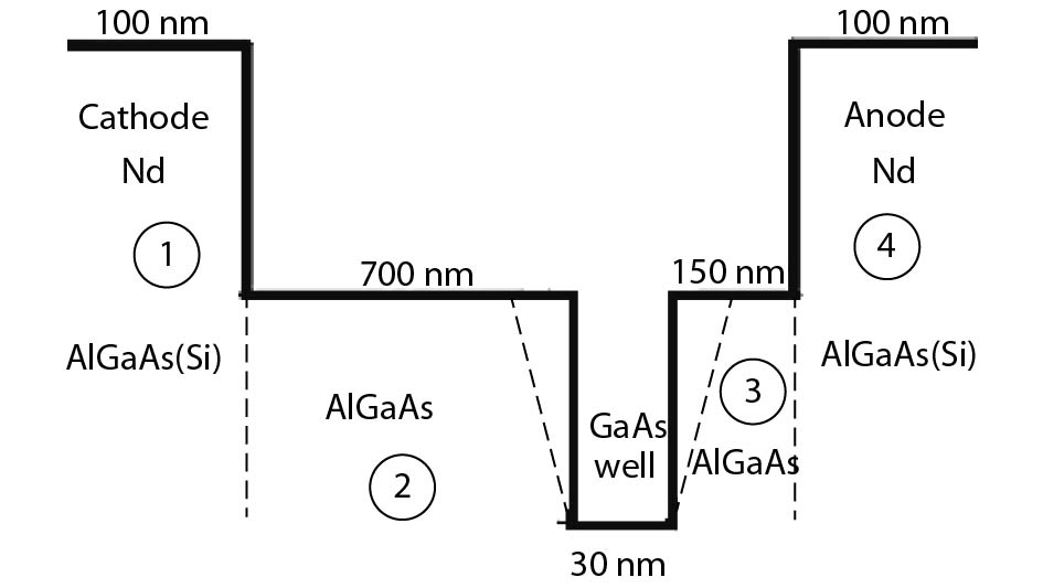
The experimental set up and procedures have been reported in Refs. [1, 10] though, a summary of the experiments will be described in this paper too. We consider importantly the layer design and growth process to realize diodes with low voltage detection capability. The epitaxial structure of the devices used for this investigation was a GaAs/AlGaAs heterostructure as shown in Fig. 1. This structure contains doped n+ regions of Al0.3Ga0.7As(Si), 100 nm long and doping concentration of 4.10 × 1024 m–3 on both diode terminals (labels 1 and 4) which interact with the ohmic contacts. Labels 2 and 3 represent the left and right intrinsic regions of Al0.3Ga0.7As with lengths 7000 and 1500 Å respectively, while a GaAs well of width 300 Å was inserted between the two intrinsic regions. The experiment was done under tight control required over the thickness and composition of each epitaxial layer and performed in a RIBER V90H reactor on n+ GaAs substrates. Circular diode with diameter 50 μm was fabricated using i-line optical lithography in a standard wet etched process. The front and back contacts, consisting of 50 nm AuGe/13 nm Ni/200 nm Au were thermally evaporated and annealed providing a very low contact resistance. This was followed by an orthophosphoric based etch to produce self-aligned mesas to a depth of 1.5 μm using the top contact metal as a mask. Measurements of device were carried out on-wafer using a probe station at room temperature. The device I–V characteristics were measured using an Agilent (keysight) B1500A Semiconductor Device Analyser from –3 to 2 V.
![]()
Figure 1.The epitaxial structure of the potential well barrier diode showing all the design parameters.
3. The Monte Carlo model
The Monte Carlo model used here was initially developed to study the transport formalism in semiconductor devices and has been used extensively to study operation of the Gunn diodes[
4. Results and discussion
4.1. Comparison of diode I–V characteristics using experimental results, MC and DD models.
Fig 2 shows the comparison of the I–V characteristics of the PWB diode using the Monte Carlo (solid line), drift-diffusion (dotted line) models and the experimental data (diamond) for the same nominal structure. Both models seem to agree with each other fairly well at low currents, especially up to a bias of 0.3 V but give quite different results at higher currents. This is obviously due to decreases in carrier mobility since carrier heating effect dominates the device by the large electric fields. Though sensitivity to variation in parameters was investigated in Ref. [10] and it was only with fitting to parameters that the DD simulation model agreed well with experimental I–V characteristics as reported in Ref. [10].
![]()
Figure 2.Comparison of the experimental results (diamond), the drift-diffusion (broken line) and Monte Carlo (solid line) simulation models. Result shows that the MC model has better agreement with the experimental results than the DD model lower bias (a) linear (b) logarithmic plots.
However, for the same nominal values of parameters as the experimental device, we observed that there is a better agreement with the MC model especially at current densities more than 0.5 μA/m2 (though noise in the MC model makes determining currents below 0.3 V difficult) but the DD simulation model significantly overestimates the current for biases above 0.3 V since the DD treats electron mobility of carriers as being in equilibrium with the field at a constant temperature. Also, in the DD models, the electron gas is assumed to be in thermal equilibrium with the lattice temperature. In the presence of a strong electric field however, electrons gain energy from the field and the temperature of the electron gas is increased further. Thus, electron transport is influenced by pressure gradient rather than just density gradient since the pressure of electron gas is proportional to nkBTn[
The differences between the MC and DD models are primarily due to reduction in carrier mobility in the MC model as a result of carrier heating in the active region of diode by large electric fields as suggested by Ref. [7] for PDB’s. The lowering of the current density due to carrier heating is also caused by back scattering of hot electrons in the anode (collector) region of the diode which also decreases the net current over the barrier in the MC model as in Ref. [7]. Carrier heating occurs in the PWB diode due to energy exchanges that occur between the electrons and lattice due to phonons especially, when the electric field is so high enough to exceed velocity saturation[
However, unlike in a PDB, there would seem to be a small reduction in the potential barrier in the PWB diode due to a reduction of carriers in the well because of higher temperatures. This to a certain extent mitigates the differences in current between the two models that would be expected in a PDB.
4.2. Influence of bias on the electric field
Fig. 3 shows the variation of the effective electric field with applied bias as simulated by the MC model.
![]()
Figure 3.Behaviour of effective (including the band offset) electric field for various operating bias across the diode.
The large electric field changes rapidly over the length of the device as the applied bias increases thus, creating non-local and hot carrier effect which dominates the performance of the device. There is however a sudden rise in the effective field at the right edge of the potential well at a position of 1 μm across the diodes as the field receives a boost due to the high energy acquired in the potential well.
4.3. Electron population in the Г-valley
As shown in Fig. 4, the population of the electrons across the diode varies with changes in the applied bias. As electric field increases across the diode due to increases in the applied bias, this significantly increases the speed of electrons in the lower valley as electrons get heated up and become more excited. As a result, electrons gain significant energy even beyond acoustic phonon thus, intervalley transfer rapidly increases and the gamma valley population reduces significantly with such high electric field. Fig. 4 shows decreases in the percentage of charge in the Г-valley across the diode. For example at a distance of 1.08 μm (to the right of the diode), the estimated percentage population of electrons at this position for 0.5, 1.0 and 2.0 V respectively are 52.4%, 24.47% and 14.06%. Also in the well at a position between 0.98 and 1.01 μm, the respective estimated percentage of electrons in the gamma valley for biases of 0.5, 1.0 and 2.0 V is 74.12%, 50.04% and 32.5 %.
![]()
Figure 4.Effect of varying electric field on the population of electron across the diode. The result shows that there are more electrons in the diode operating at a lower field (bias of 0.5 V).
4.4. Comparison of the mean electron velocity
The velocity of electrons is one of the most important parameter used for characterizing the microscopic quality of semiconductors[
![]()
Figure 5.Electron velocity as a function of positon across the diode under influence of non-stationary field. Results shows little differences in the maximum velocity for the three biases: 0.5, 1.0 and 2.0 V. The velocity drops faster across the diode for diode operating at 2.0 V.
This shows how the electrons at higher bias across the diode saturate faster compared to electrons at lower bias. The most important point we wish to stress here is that, a higher bias results to higher electric field and this initially increases the mobility of the electrons in the device. There is therefore a tendency of achieving a high frequency with PWB diodes operating with high electric field though, frequency operation not considered here in this study.
4.5. Effect of bias on the mean electron energy
Fig. 6 shows that the electrons across the diode get hotter as the bias increases and causes the average kinetic energy to increase. The results shown in Fig. 6 are similar in form to those observed in Ref. [7] for PDB’s. For a bias of 0.5 V, the diode maintained a nearly constant energy of approximately 0.041 eV up to a distance of 0.35 μm. Thus, the average kinetic energy starts increasing steadily until it reaches a maximum value of 0.068 eV at position of 1.0 μm across the diode.
![]()
Figure 6.Average electron energy as function of position across diode for several bias. The mean energy of electrons increases considerably with the bias.
For the bias of 2.0 V the electron energy rises steadily from a position of 0.25 μm up to 0.078 eV at the edge of the well. The kinetic energy abruptly increases to 0.11 eV where it reaches a peak in the right intrinsic region (at position of 1.12 μm across diode). For an applied bias of 1.0 V, the mean kinetic energy lies intermediate between the kinetic energy of applied bias of 0.5 and 2.0 V. The average kinetic energy of electrons at this bias increases steadily from position of 0.32 μm and peaks at position of 1.09 μm with a value of 0.08 eV. This result shows that at a higher applied bias, more inter-valley scattering from the Г–valley to the composite heavy valleys occurs hence, causing greater hot electron effects in the diode compared to lower biases. The average kinetic energy across the diode reflects the applied bias and is similar in form to a PDB[
5. Conclusion
In conclusion, the application of Monte Carlo model in the study of hot carrier effects in PWB diodes provides a good understanding of interior carrier transport of these devices and also gives a better description and a quantitative analysis of high and low current operation in these diodes. The I–V characteristics values produced by the Monte Carlo model are lower than those predicted by DD models and in better agreement with the experimental results due to reduction in the mobility of carriers because of hot carrier effects. Results of the I–V characteristics of the conventional DD models demonstrate the limitation of the model to predicting some of the important diode’s attributes. Also, the MC model was used to investigate the behavior of the PWB diode to changes in operating bias in terms of the mean kinetic energy of electrons, average electron velocity, population of charge across device and electric field distribution across diode active region thus, demonstrating the importance of the hot carrier model in the diode analysis. There are of course uncertainties in the epitaxial structure and fabrication of these devices which make the experimental results uncertain and hence any conclusions that we can draw. However, the consistently better agreement between experiment and the MC model which includes hot carrier effects over the DD model which did not include such effects, provides compelling evidence for the importance of hot electron effects in these devices.
Acknowledgements
This work was supported by the College of Physical Sciences, University of Aberdeen, UK.
References
[1] M Akura, G Dunn, J Sexton et al. Potential well barrier diodes for submillimeter wave and high frequency applications. IEEE Electron Device Lett, 38, 438(2017).
[2] R J Malik, T R Aucoin, R L Ross et al. Planar-doped barriers in GaAs by molecular beam epitaxy. Electron Lett, 16, 836(1980).
[3] S Dixon, R Malik. Subharmonic planar doped barrier mixer conversion loss characteristics. IEEE Trans Microwave Theory Tech, 31, 155(1983).
[4]
[5] M Akura, G Dunn, M Missous. A hybrid planar-doped potential-well barrier diode for detector applications. IEEE Trans Electron Devices, 64, 4031(2017).
[6] E Kollberg, L Rydberg. Quantum barrier varactor diodes for high efficiency millimetre-wave multipliers. Electron Lett, 25, 1696(1989).
[7] R K Cook. Computer simulation of carrier transport in planar doped barrier diodes. Appl Phys Lett, 42, 439(1983).
[8] N R Couch, M J Kearney. Hot electron properties of GaAs planar doped barrier diodes. J Appl Phys, 66, 5083(1989).
[9] T Wang, K Hess, G J Lafrate. Time-dependent ensemble Monte Carlo simulation for planar doped GaAs structures. J Appl Phys, 58, 857(1985).
[10] M Akura, G Dunn, J Sexton et al. GaAs/AlGaAs potential well barrier diodes: Novel diode for detector and mixer applications. Phys Status Solidi A, 214, 17002901(2017).
[11] M Akura, G Dunn. Investigating the effect of temperature on barrier height of PWB diodes. Electron Lett, 54, 42(2017).
[12] M Akura, G Dunn, M Missous. Investigating the role of band offset on the property and operation of the potential well barrier diodes. Phys Status Solidi B, 256, 1800284(2019).
[13] Tuyen V Van, B Szentpa'li. Tunneling in planar-doped barrier diodes. J Appl Phys, 68, 2824(1990).
[14] W N Jiang, U K Mishra. Current flow mechanisms in GaAs planar-doped-barrier diodes with high built-in fields. J Appl Phys, 74, 5569(1993).
[15] J Liberis, A Matulionis, P Sakalas et al. Noise in physical systems and 1/
[16] C Li, A Khalid, N Piligrim et al. Novel planar Gunn diode operating in fundamental mode up to 158 GHz. J Phys: Conf Ser, 193, 0120291(2009).
[17] T Teoh, G Dunn, N Priestley et al. Monte Carlo modelling of multiple-transit-region Gunn diodes. Semicond Sci Technol, 17, 1090(2002).
[18] N Pilgrim, R Macpherson, A Khalid et al. Multiple and broad frequency response Gunn diodes. Semicond Sci Technol, 24, 105010(2009).
[19] J C Jacoboni, L Reggiani. The Monte Carlo method for the solution of charge transport in semiconductors with applications to covalent materials. Rev Mod Phys, 55, 645(1983).
[20] W Fawcett, A D Boardman, S Swain. Monte Carlo determination of electron transport properties in gallium arsenide. J Phys Chem Solids, 31, 1963(1970).
[21] R W Hockney, J W Eastwood. Computer simulation using particles. Bristol and Philadelphia: CRC Press, 374(1988).
[22] K Tomizawa. Numerical simulation of submicron semiconductor devices. London: Artech House, 115(1993).
[23]
[24] C M Snowden. Semiconductor device modelling. London: Peter Peregrinus Ltd, 5, 175(1988).
[25] T Grasser, T Tang, H Kosina et al. A review of hydrodynamic and energy transport models for semiconductor device simulation. Proc IEEE, 91, 251(2003).
[26]
[27] J Frey. Where do hot electrons come from. IEEE Circuits Devices Mag, 7, 31(1991).
[28]

Set citation alerts for the article
Please enter your email address
© Copyright 2018-2021 | Chinese Laser Press. All Rights Reserved 沪ICP备15018463号-20