• Infrared and Laser Engineering
  • Vol. 52, Issue 5, 20220838 (2023)
Xin Zhang1, Le Zhang1,*, Chi Song2,*, Lisong Yan3..., Xiaolin Yin1 and Binzhi Zhang1|Show fewer author(s)
Author Affiliations
  • 1JiHua Laboratory, Foshan 528200, China
  • 2School of Mechatronic Engineering and Automation, Foshan University, Foshan 528225, China
  • 3School of Optical and Electronic Information, Huazhong University of Science and Technology, Wuhan 430074, China
  • show less
    DOI: 10.3788/IRLA20220838 Cite this Article
    Xin Zhang, Le Zhang, Chi Song, Lisong Yan, Xiaolin Yin, Binzhi Zhang. Study on surface roughness of monocrystalline silicon carbide based on PSD evaluation and pseudo-random tool path[J]. Infrared and Laser Engineering, 2023, 52(5): 20220838 Copy Citation Text show less
    References

    [1] Liting Li. Research progress of silicon carbide semiconductor materials and suggestions for its industrial development. Xiamen Science & Technology, 1-11(2016).

    [2] Keyun Bi, Songfa Li. The development of wide band gap semiconductor device. Journal of Caeit, 1, 6-10(2016).

    [3] A A Lebedev, V E Chelnokov. Wide-gap semiconductors for high-power electronics. Semiconductors, 33, 999-1001(1999).

    [4] H Lendenmann, J P Bergman, F Dahlquist, et al. Degradation in SiC bipolar devices: Sources and consequences of electrically active dislocations in SiC. Materials Science Forum, 433, 901-906(2003).

    [5] Xu Wang. Evaluation of the RB-SiC mirror surface fabricated with the fixed abrasive technology. Infrared and Laser Engineering, 41, 2074-2479(2012).

    [6] Zhuolin Li, W B Lee. Study on removal characteristic of silicon carbide surface in precision mechanical polishing. Infrared and Laser Engineering, 45, 0220003(2016).

    [7] Lingzhong Li, Xiaokun Wang, Erhui Qi, et al. Research status analysis of subsurface damage characterization and measurement technology of optical components (invited). Infrared and Laser Engineering, 51, 20220572(2022).

    [8] Shang Gao, Tianrun Li, Hongye Lang, et al. Prediction for subsurface damage depth of silicon wafers in workpiece rotational grinding. Optics and Precision Engineering, 30, 2077-2087(2022).

    [9] G Wenski, T Altmann, W Winkler, et al. Doubleside polishing—a technology mandatory for 300 mm wafer manufacturing. Materials Science in Semiconductor Processing, 5, 375-380(2002).

    [10] Everson W J, Snyder D, Heydemann V D. Polishing surface acterization of SiC substrates[C]Materials Science Fum, 2000.

    [11] G S Lee, H H Hwang, C H Son, et al. The effect of slurry composition and flatness on sub-surface damage and removal in chemical mechanical polishing of 6H-SiC. Materials Science Forum, 615-617, 605(2009).

    [12] Shouzhen Jiang, Xiangang Xu, Juan Li, et al. Recent progress in SiC monocrystal growth and wafer machining. Chinese Journal of Semiconductor, 28, 810-814(2007).

    [13] Dongming Guo, Renke Kang, Jianxiu Su, et al. Future development on wafer planarization technology in ulsi fabrication. Chinese Journal of Mechanical Engineering, 39, 100-105(2003).

    [14] G S Pan, Z H Gu, Y Zhou, et al. Preparation of silane modified SiO2 abrasive particles and their Chemical Mechanical Polishing (CMP) performances. Wear, 273, 100-104(2011).

    [15] Yan Zhou, Guoshun Pan, Xiaolei Shi, et al. Chemical Mechanical Planarization (cmp) of on-axis si-face sic wafer using catalyst nanoparticles in slurry. Surface & Coatings Technology, 43, 42-47(2021).

    [16] Song Chi. Fabrication of large aspherics using nonNewtonian fluid polishing tool [D]. Beijing: University of Chinese Academy of Sciences, 2017. (in Chinese)

    [17] H Y Li, W David, G Y Yu, et al. Modeling and validation of polishing tool influence functions for manufacturing segments for an extremely large telescope. Appl Opt, 52, 5781-5787(2013).

    [18] Mingze Li, Xi Hou, Wenchuan Zhao, et al. Current situation and development trend of aspheric optical surface defect detection technology (invited). Infrared and Laser Engineering, 51, 20220457(2022).

    [19] Zijian Liang, Yongying Yang, Hongyang Zhao, et al. Advances in research and applications of optical aspheric surface metrology. Chinese Optics, 15, 161-186(2022).

    [20] Yaru Wang, Yingjie Li, Lai Zou, et al. Material removal and surface damage behavior of diamond grain for flexible scribing RB-SiC. Optics and Precision Engineering, 30, 1704-1715(2022).

    [21] Zhanlong Ma, Junlin Wang. Ultra-precision optical fabrication technology. Infrared and Laser Engineering, 42, 1485-1490(2013).

    [22] Xuefeng Zeng, Xuejun Zhang. Impact of mid-spatial frequency errors in optical manufacturing on modulation transfer function. Laser & Optoelectronics Progress, 52, 232-237(2015).

    [23] Li Qi. Study on stability improvement path optimization in numerical control small tool polishing f optical component [D]. Changsha: National University of Defense Technology, 2014. (in Chinese)

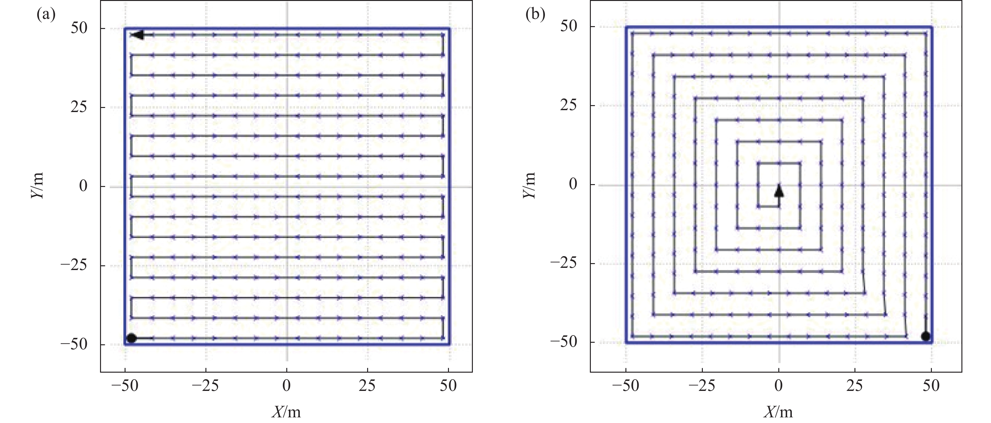
    Xin Zhang, Le Zhang, Chi Song, Lisong Yan, Xiaolin Yin, Binzhi Zhang. Study on surface roughness of monocrystalline silicon carbide based on PSD evaluation and pseudo-random tool path[J]. Infrared and Laser Engineering, 2023, 52(5): 20220838
    Download Citation