
Qingyang Du, Jérôme Michon, Bingzhao Li, Derek Kita, Danhao Ma, Haijie Zuo, Shaoliang Yu, Tian Gu, Anuradha Agarwal, Mo Li, Juejun Hu, "Real-time, in situ probing of gamma radiation damage with packaged integrated photonic chips," Photonics Res. 8, 186 (2020)
- Photonics Research
- Vol. 8, Issue 2, 186 (2020)
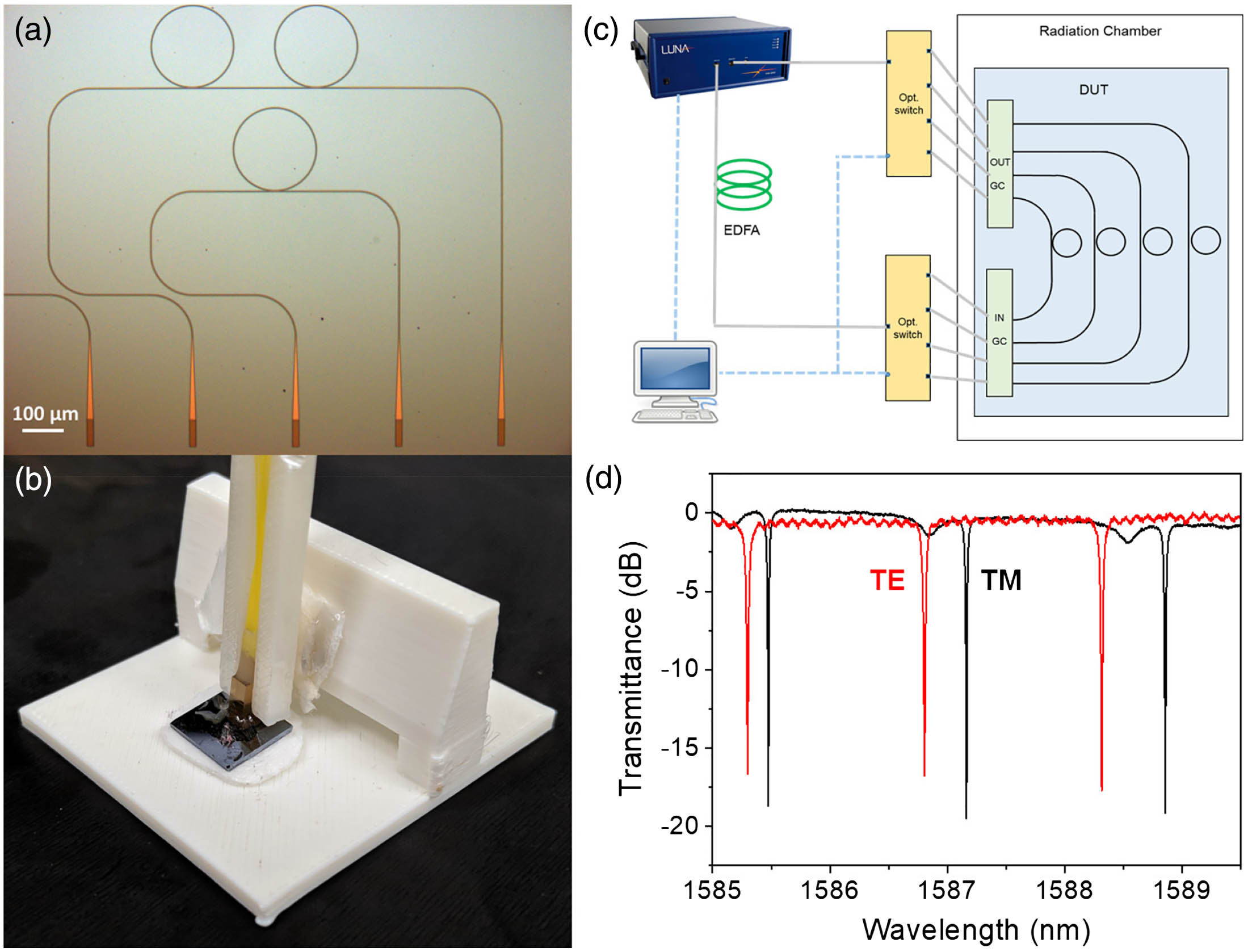
Fig. 1. (a) Top-view micrograph of the photonic chip showing the micro-ring resonators and the grating couplers; (b) photograph of the packaged photonic chip; (c) block diagram showing the in situ measurement setup. EDFA, erbium-doped fiber amplifier; GC, grating coupler; Opt. switch, optical switch; DUT, device under test. (d) Normalized transmittance spectra of a micro-ring resonator under test for both TE- and TM-polarized modes.
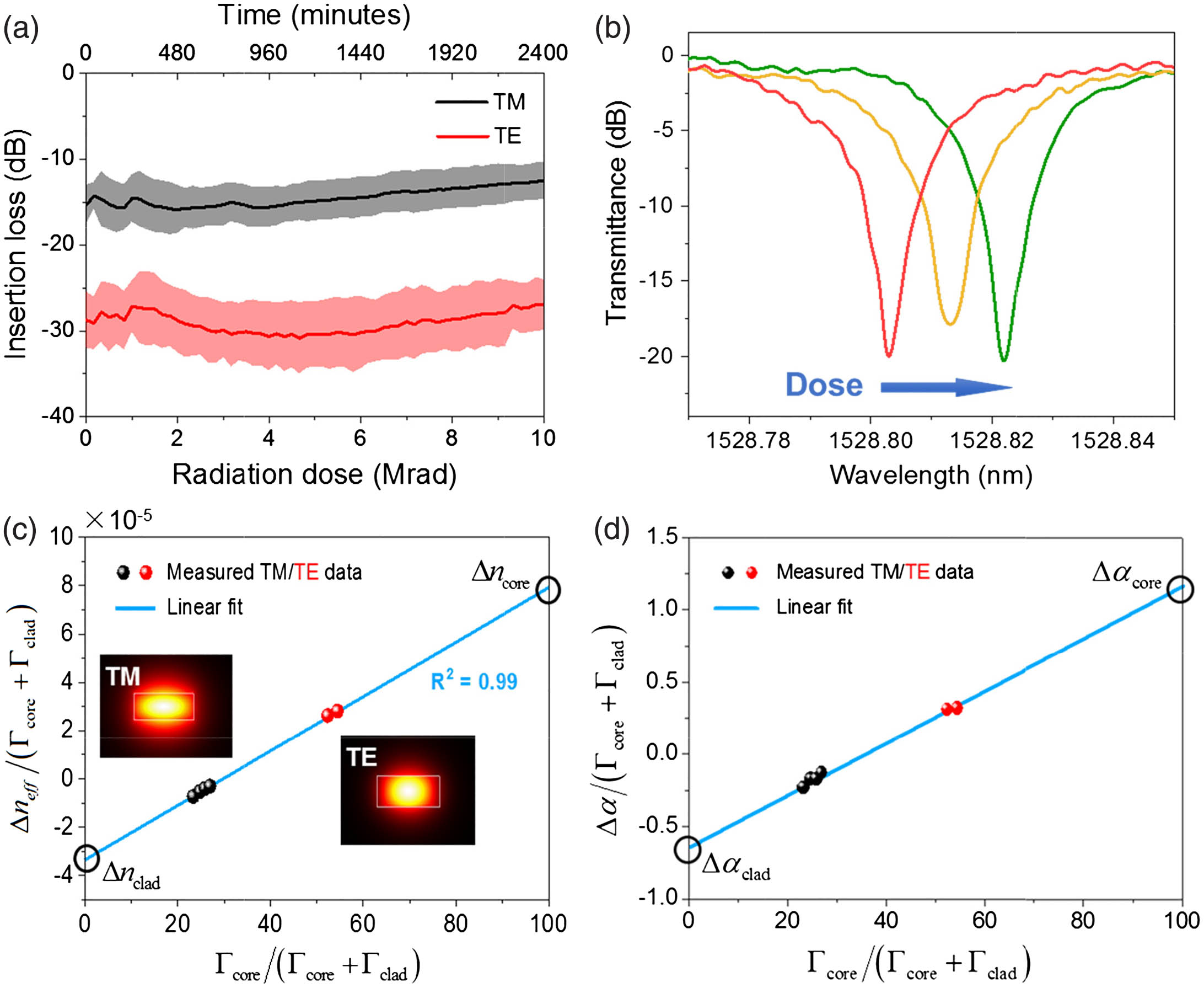
Fig. 2. (a) Insertion loss change of the fiber-packaged chip during in situ irradiation: here the error bars (shaded regions) are defined as the device-to-device variations on the same chip; (b) resonance shift due to gamma irradiation; the three spectra correspond to 0, 3.6 Mrad, and 8.4 Mrad radiation doses, respectively; (c) extracting material index changes from device measurements following protocols described in the text. The insets show TE- and TM-polarized waveguide mode profiles for SiC waveguides; (d) extracting material loss change from device measurement.
Fig. 3. In situ measured changes of (a) refractive indices and (b) optical losses in SiC and SiO 2
Fig. 4. Post-irradiation relaxation of (a) refractive indices and (b) optical losses in SiC and SiO 2
Fig. 5. SIMS elemental depth profiles of (a) as-deposited and (b) irradiated a-SiC films.
|
Table 1. Calculated Displacement Damage Parameters in a-SiC at 10 Mrad Radiation Dose


Set citation alerts for the article
Please enter your email address

© Copyright 2018-2021 | Chinese Laser Press. All Rights Reserved 沪ICP备15018463号-20