Integrated photonics is poised to become a mainstream solution for high-speed data communications and sensing in harsh radiation environments, such as outer space, high-energy physics facilities, nuclear power plants, and test fusion reactors. Understanding the impact of radiation damage in optical materials and devices is thus a prerequisite to building radiation-hard photonic systems for these applications. In this paper, we report real-time, in situ analysis of radiation damage in integrated photonic devices. The devices, integrated with an optical fiber array package and a baseline-correction temperature sensor, can be remotely interrogated while exposed to ionizing radiation over a long period without compromising their structural and optical integrity. We also introduce a method to deconvolve the radiation damage responses from different constituent materials in a device. The approach was implemented to quantify gamma radiation damage and post-radiation relaxation behavior of -cladded SiC photonic devices. Our findings suggest that densification induced by Compton scattering displacement defects is the primary mechanism for the observed index change in SiC. Additionally, post-radiation relaxation in amorphous SiC does not restore the original pre-irradiated structural state of the material. Our results further point to the potential of realizing radiation-hard photonic device designs taking advantage of the opposite signs of radiation-induced index changes in SiC and .
1. INTRODUCTION
Over the past decade, integrated photonics has rapidly been established as the technology of choice over electronics for applications covering long-haul data communications [1], radio-frequency photonics [2], and on-chip spectroscopic sensing [3]. Devices for operation in harsh radiation environments are yet another arena where integrated photonics presents unique advantages. Integrated photonic modules are being deployed in these settings for applications including optical links for high-volume high-energy physics data transmission [4] and satellite communications [5]. In addition to their inherent advantages in energy-efficient data communications and remote sensing/imaging, recent studies have revealed that various radiation-hard integrated photonic components can be realized with proper designs [6–9].
To enable such radiation-hard designs, it is essential to develop a thorough understanding of the radiation-induced effects in relevant photonic materials and devices. Toward this goal, several studies have been undertaken to evaluate the effects in integrated photonic devices [10–14]. In these studies, responses of the devices to ionizing radiations were only quantified ex situ, i.e., after the devices were removed from the irradiation chamber. On the other hand, in situ monitoring of radiation damage has also been reported in silicon-on-insulator micro-ring resonators (under gamma ray irradiation) [15] and Mach–Zehnder interferometers (under X-ray and neutron irradiation) [16,17]. Such measurements allow for real-time monitoring of the kinetics of radiation damage as well as post-radiation relaxation, which takes place at room temperature and commences immediately after irradiation concludes [18,19].
A standing challenge, however, is that only radiation-induced changes of the overall device response were reported in these studies, and it is unclear which constituent materials are responsible for the performance variation and to what extent. For instance, in an optical waveguide, both the core and cladding materials influence its optical properties; elucidating their respective relative contributions can open up engineering spaces for radiation-hard designs, as we shall discuss later. It is therefore imperative to identify a technique to deconvolve the radiation-induced responses of individual constituent materials.
Sign up for Photonics Research TOC. Get the latest issue of Photonics Research delivered right to you!Sign up now
In this study, we seek to address the challenge by performing real-time measurements of photonic device arrays while they were being irradiated in situ. Stable long-term measurements were made possible by packaging the devices with optical fiber arrays (FAs) as a robust optical interface for light input/output coupling. We further leverage the FAs to facilitate parallel characterization of multiple waveguide devices on the same chip. The devices, each designed with a different geometric dimension, give rise to distinctive field distributions in the core and cladding materials. The difference in their radiation-induced responses was then used to isolate the property changes of the core and cladding materials.
2. DEVICE FABRICATION AND PACKAGING
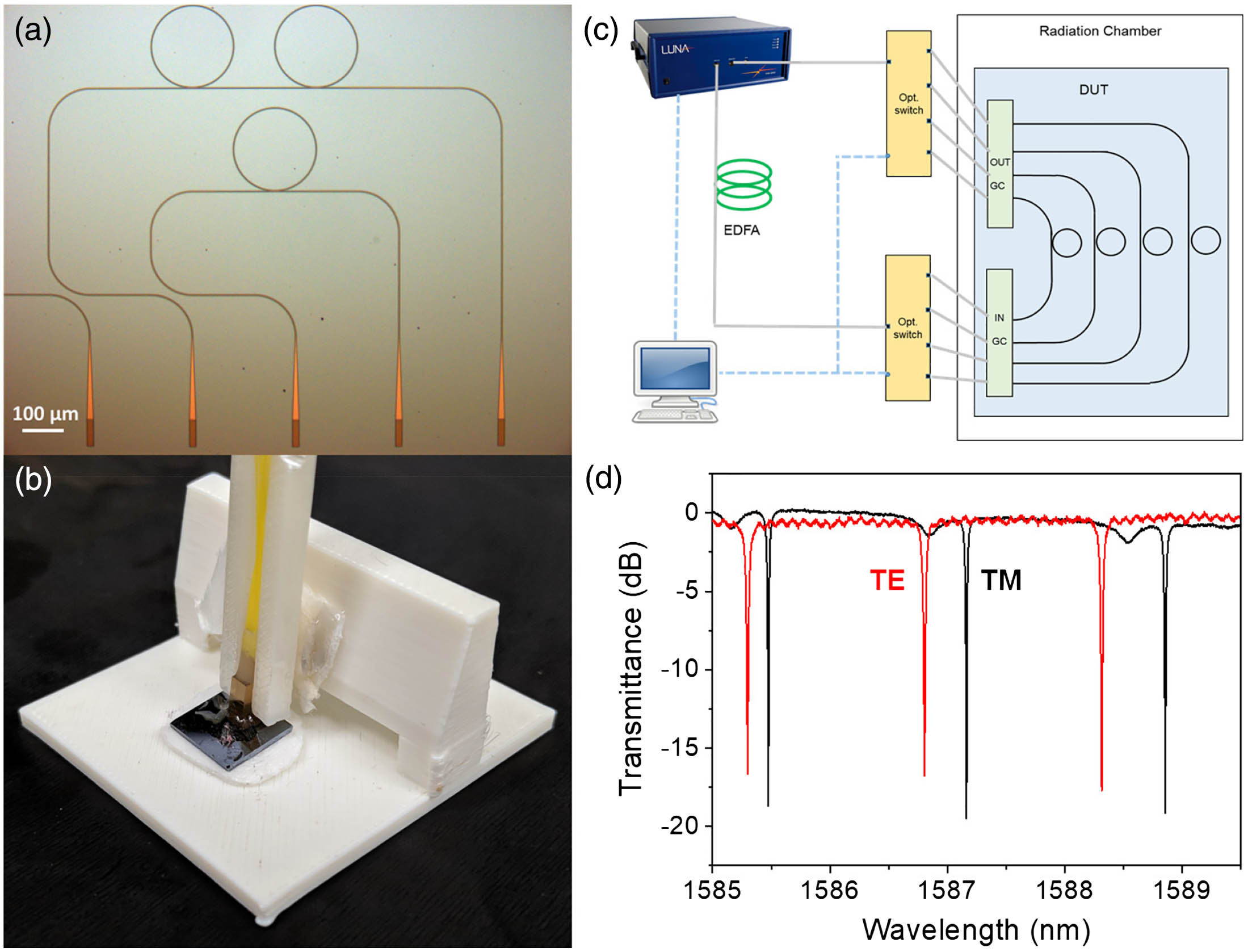
Specifically, we employ as the model system to demonstrate our approach. SiC, which consists of a robust 3D covalent atomic network interconnected through strong Si-C bonds, has long been regarded as a leading material candidate for radiation-hard devices [20]. Recently, there has been a surge of interest in SiC for integrated photonics applications covering non-linear optics, optomechanics, and quantum optics [20–34]. In our study, we choose amorphous SiC (a-SiC) deposited using plasma-enhanced chemical vapor deposition (PECVD) as the material platform. The choice of PECVD SiC as the waveguide core material is mainly justified by its CMOS compatibility and ease of processing [21,22], as neither wafer bonding (in the case of SiC-on-insulator) [23–25] nor undercut etching for suspended structures (in the case of epitaxial SiC-on-Si) [26–34] is needed. The devices were fabricated on piranha cleaned Si wafers. The process started with growing a 2-μm-thick PECVD under cladding layer. A 275-nm film of amorphous silicon carbide was deposited subsequently via PECVD with a gas mixture of and following previously published conditions [22]. Patterning of the SiC film was conducted on an Elionix ELS-F125 electron beam lithography (EBL) tool with a beam current of 10 nA and an optimized dose of μ. 6% hydrogen silsesquioxane was chosen as the EBL resist as it provides optimal etching resistivity. The chip was then developed in 25% tetramethylammonium hydroxide for 2.5 min to reveal the pattern. Reactive ion etching was performed in an STS inductively coupled plasma reactive ion etching tool (ICP-RIE) with a forward power of 1000 W and an etching gas of at a pressure of 30 mTorr. These parameters yielded an etching rate of a-SiC at 600 nm/min. Device fabrication was completed by depositing another 2-μm PECVD oxide layer as the top cladding. The devices fabricated following the protocols are symmetrically cladded with PECVD . The cross-sectional dimensions of the waveguides were quantified using scanning electron microscopy and used as input parameters for full-vectorial optical modal simulations. In device packaging, the as-fabricated devices were packaged with optical fiber arrays (SQS Vlaknova Optika) using UV curable epoxy (Masterbond UV15TK) as the bonding agent. Fibers with an incident angle of 15° were first actively aligned to the on-chip grating couplers to maximize the transmitted power. Epoxy was applied onto the chip to securely bond the fibers to the chip. The active alignment was repeated after epoxy application to ensure optimal coupling. The epoxy was then cured through flood UV exposure. After the epoxy was fully cured, the fibers were released from the alignment stage and attached to a custom-designed and 3D printed device holder. A thermal couple is also bonded onto the chip for in situ temperature monitoring. Figure 1(b) shows an image of the packaged photonic chip. Prior to irradiation, the temperature-dependent wavelength shifts of the SiC resonator devices under test were quantified and used to correct the resonance drift due to ambient temperature fluctuations during the experiment. The fiber-tethered devices were then loaded into a GammaCell Co-60 Irradiator and exposed to a gamma ray dose rate of approximately 4000 rad/min (calibrated with respect to Si). Transmittance spectra of both transverse electric (TE) and transverse magnetic (TM) polarizations were recorded concurrently using an optical vector analyzer (LUNA Technologies OVA-5000) with a built-in external cavity tunable laser. Figure 1(c) depicts a block diagram illustrating the testing setup and a representative set of measured TE/TM spectra is shown in Fig. 1(d).
Figure 1.(a) Top-view micrograph of the photonic chip showing the micro-ring resonators and the grating couplers; (b) photograph of the packaged photonic chip; (c) block diagram showing the in situ measurement setup. EDFA, erbium-doped fiber amplifier; GC, grating coupler; Opt. switch, optical switch; DUT, device under test. (d) Normalized transmittance spectra of a micro-ring resonator under test for both TE- and TM-polarized modes.
Long-term stability of the fiber package under gamma irradiation was experimentally confirmed by examining the loop-back insertion loss variation in the in situ experiment. As is shown in Fig. 2(a), changes of the insertion losses remain negligible up to a large irradiation dose of 10 Mrad and are consistently less than the device-to-device variation. On the device side, gamma ray irradiation resulted in progressive resonant wavelength shifts with increasing dose [Fig. 2(b)]. The observed resonant wavelength shift was a combined effect of radiation-induced refractive index changes in the SiC core () and cladding (). To elucidate the respective contributions from the core and cladding, micro-ring resonators with different core widths (from 700 nm to 1000 nm) but otherwise identical configurations (275 nm core height, 150 μm diameter) were fabricated on the same chip. Waveguides with different dimensions give rise to varying confinement factors and in the core and cladding regions, respectively. The measured resonant wavelength drift relates to the modal effective index change caused by irradiation through Here denotes the starting resonant wavelength and is the group index. It is important to note that and in general do not add up to unity due to the slow light effect [35]. We define normalized confinement factors as follows: We see that the sum of the so-defined and always equals unity. Equation (1) can then be cast in the following form: Equation (3) suggests that the measured for all the resonators and polarizations at a given radiation dose, when plotted as a function of , should fall on a straight line. As is seen in an example shown in Fig. 2(c), this is indeed the case and linear fits of our measured data consistently give coefficients of determination () above 0.99. The intercepts of the fitted line with and then correspond to and , respectively, with the particular radiation dose.
Figure 2.(a) Insertion loss change of the fiber-packaged chip during in situ irradiation: here the error bars (shaded regions) are defined as the device-to-device variations on the same chip; (b) resonance shift due to gamma irradiation; the three spectra correspond to 0, 3.6 Mrad, and 8.4 Mrad radiation doses, respectively; (c) extracting material index changes from device measurements following protocols described in the text. The insets show TE- and TM-polarized waveguide mode profiles for SiC waveguides; (d) extracting material loss change from device measurement.
Besides inferring the index changes of core and cladding materials, the same notion can also be applied to extract the optical loss variations in both materials from the quality factor (-factor) modifications of the different resonator devices and polarizations and is shown in Fig. 2(d). The detailed formalism of the extraction procedure is presented in Appendix A.
Figures 3(a) and 3(b) plot the radiation-dose-dependent changes in material refractive indices and optical losses, respectively. Optical losses in the materials hardly changed within the measurement error throughout the course of the irradiation experiment. The relatively large spread in the measured optical losses () is attributed to inherent scattering loss variations in micro-ring resonators [36]. In contrast, refractive index changes ranging from to were unambiguously quantified taking advantage of the extreme precision afforded by resonant cavity refractometry [37–39]. This index drift is sufficiently small to be negligible for most guided wave devices. However, in devices sensitive to optical phase variations, such as Mach–Zehnder interferometers and resonators, this index drift must be properly compensated. It is also interesting to note that SiC and exhibit index changes with opposing signs. This observation implies the possibility of creating radiation-hard optical devices by engineering modal confinement to nullify the effective index drift. One such hypothetical design is illustrated in Fig. 3(c), and the projected dose-dependent effective index change of the device is plotted in Fig. 3(d) based on the measured index change values in Fig. 3(a). The design predicts waveguide effective index drift of less than , more than an order of magnitude smaller than the index changes of SiC or alone. Such a design is useful in improving phase stability of photonic components in radiation environments.
Figure 3.In situ measured changes of (a) refractive indices and (b) optical losses in SiC and induced by gamma ray irradiation; (c) TE mode intensity profile of the radiation-hard SiC waveguide device design; (d) projected TE-mode effective index change of the design in (c) based on measurement data in (a). The shaded regions in (a), (b), and (d) denote standard deviations of data taken on multiple devices on the same chip.
The packaged device also facilitates real-time tracking of the materials’ post-radiation relaxation response at room temperature. Figures 4(a) and 4(b) plot the index and loss relaxation behavior of SiC and after 10-Mrad irradiation. While the loss variation is insignificant, we observed considerable index change in SiC. Remarkably, the post-radiation index change in SiC over time is non-monotonic, showing an initial increase followed by a decrease. This is in contrast to the refractive index relaxation in crystalline Si, which occurs immediately after irradiation and always rescinds the index change induced by radiation [15].
Figure 4.Post-irradiation relaxation of (a) refractive indices and (b) optical losses in SiC and . The shaded regions in (b) denote standard deviations of data taken on multiple devices on the same chip.
The results from our in situ measurement outlined above provide important insights into the mechanism of radiation damage in a-SiC for photonic applications. In general, there are three possible damage mechanisms caused by gamma radiation which can lead to optical property modifications: (1) ionizing radiations generate electron and hole pairs which introduce free carrier absorption and refractive index change through the plasmon dispersion effect [40]; (2) high-energy photons or particles can catalyze oxidation reactions. For instance, gamma radiation was reported to induce surface oxidation and refractive index change in SiN and a-Si when the samples were exposed to an ambient environment [11]; and (3) while direct momentum transfer from the photons of gamma rays to atoms is minimal, high-energy electrons emitted through the Compton scattering process can collide with atoms and produce point (displacement) defects [41]. Formation of these point defects further triggers a drastic rise in local temperature and pressure, which prompts local network configuration and density change in an amorphous material [42].
Here we argue that volume compaction due to Compton scattering displacement is the main mechanism responsible for the observed change in SiC. In a-SiC, the free carrier effects are negligible due to low carrier concentration and their mobility. In addition, the persistent index change after the removal of the sample from the irradiation chamber can hardly be accounted for by free carrier effects. Our SiC devices are entirely encapsulated in a cladding and isolated from the ambient atmosphere. Moreover, to identify possible radiation-induced chemical modifications in a-SiC, we performed secondary ion mass spectroscopy (SIMS) analysis on a-SiC thin films before and after 10-Mrad total dose gamma irradiation. As is evident from Fig. 5, PECVD-deposited a-SiC film contains a high concentration of H, which is instrumental in passivating the dangling bond defects in amorphous Group IV semiconductors. An increasing oxygen concentration near the film surface indicates in-diffusion of oxygen causing surface oxidation. However, the composition profile remains identical before and after gamma irradiation, suggesting that surface oxidation is self-terminating even in uncapped a-SiC films.
Figure 5.SIMS elemental depth profiles of (a) as-deposited and (b) irradiated a-SiC films.
To further reinforce the argument, we computed the atomic displacement parameters in SiC and the results are summarized in Table 1. Details of the calculations are furnished in Appendix A. The calculated maximum atomic recoil energies are significantly larger than the displacement energy threshold in a-SiC (13 eV [43]), and thus the Compton scattered electrons have a high probability of causing displacement damage in the material. The total density of displacement defects is approximately , or per atomic site. The heat and pressure spikes produced by each displacement defect can impact a large number of nearby atoms [42] and remove excess free volume in as-deposited a-SiC through local bond rearrangement, thereby leading to the refractive index change.
To account for the non-monotonic relaxation behavior, we note that unlike crystalline materials, the structure of amorphous compounds is characterized by a large number of metastable configurations or metabasins [44]. Structural relaxation in amorphous materials is therefore an inherently complex process and does not necessarily retrace back to the starting structural state [45]. Moreover, since the a-SiC deposited by PECVD is heavily hydrogenated, the structural relaxation kinetics may be further complicated by hydrogen diffusion, which can contribute to generation or passivation of broken (dangling) bonds in a-SiC and stabilize metastable structural configurations after irradiation [46]. The exact structural origin of the post-radiation relaxation behavior will be a topic worthy of further investigations.
5. CONCLUSION
In conclusion, in this study, we developed a method to probe optical property changes of photonic materials induced by ionizing radiations through in situ photonic device measurements. We show that the photonic package is stable in the gamma radiation environment and permits long-term, real-time measurements up to a large radiation dose. The radiation-induced refractive index change in SiC is attributed to volume compaction resulting from displacement defects generated by Compton scattered electrons. We also observed a non-monotonic variation of the SiC material refractive index during room-temperature post-radiation relaxation. Finally, findings from the study further point to the potential of realizing radiation-hard passive photonic devices leveraging the opposite signs of radiation-induced refractive index changes in different materials.
Acknowledgment
Acknowledgment. The authors acknowledge the characterization and fabrication facility of MIT Center of Materials Science and Engineering and Microsystems Technology Laboratories.
APPENDIX A
Section I—Measurement of Radiation-Induced Material Loss
Propagation loss of a resonator can be experimentally evaluated with known resonant peak extinction ratio and the quality factor (). The on-resonance power transmitted through the output end of the bus waveguide in decibel is [47] where is the amplitude coupling coefficient between the resonator and bus waveguide, and is the normalized amplitude of light after traveling one round trip around the resonator. is related to waveguide linear loss by We follow the generalized coupling matrix formalism [48] to analytically solve and and determine the waveguide loss . Given the small index change, waveguide roughness scattering loss is assumed to be constant during irradiation. The waveguide loss change is then given by where and correspond to the material loss changes in a-SiC and materials, respectively. and can be derived from the measured loss variations of waveguides with different cross-sectional dimensions following the same principle as the material refractive index quantification. Specifically, and are extracted by performing a linear fit of normalized modal loss changes against normalized confinement factors for different waveguide geometries and polarizations and extrapolating the line to normalized confinement factor values of 1 and 0, respectively. It is worth noting that the error bar of the loss quantification is significantly larger than that of index measurement because of the intrinsic dispersion of -factors in waveguide resonator devices.
Section II—Displacement Defect Parameters in Gamma-Irradiated a-SiC
The dose rate of the gamma irradiator used in our experiment is calibrated with respect to Si. The total fluence of gamma photons is related to the radiation dose via [49] where is the average gamma photon energy of 1.24 MeV and is the mass absorption coefficient equaling 0.02652 for Si [50]. Substituting the numbers into Eq. (A4), we obtain a gamma fluence of for 10 Mrad (Si) total cumulative dose.
To estimate the maximum recoil energy of atoms after collision with Compton scattered electrons, we assume that the 1.24 MeV energy of gamma photons is completely transferred to electrons. As the electron energy is considerably larger than the electron rest mass, we must use the relativistic equation to calculate the atomic recoil energy from head-on collisions: where is the maximum recoil energy the scattered electron can transfer to an atom; denotes electron rest mass; is mass of the atom; and represent the speed of the electron and light, respectively; and and are defined by and . The for Si and C is calculated to be 204 eV and 476 eV, respectively.
Atomic collision with Compton scattered electrons is the dominant mechanism for displacement defect generation. The other contributions, i.e., photoelectric effect and pair production, are negligible for gamma ray energy of 1.24 eV [41]. The Compton displacement cross sections in Si and C are calculated following Oen and Holmes [51]: where is the electron recoil energy, and , corresponding to a head-on collision with the gamma incident photon, is calculated via is the cross section for producing an electron of energy per unit range of per atom. It is given by the Klein–Nishina formula [49]: where is the electron unit charge, is the electron rest energy, and is the gamma photon energy. in Eq. (A6) is the average number of electrons with an energy of determined by the following integral: Here denotes the Avogadro constant, and is the electron displacement cross section. , the electron stopping power, is expressed as [49] where is the atomic number, and represents the mean excitation potential of the atom () [52]. Finally, the displacement defect concentration is calculated using where is the total electron flux, denotes the Compton displacements cross section, and is the atomic concentration of the target atom. Assuming an a-SiC film density of (using the bulk value) and taking into the atomic ratio of Si and C obtained from SIMS analysis, the atomic concentrations of Si and C are calculated to be and . The displacement defect concentration is then obtained using Eq. (A11). We note that PECVD-deposited a-SiC likely has a smaller density than bulk crystalline SiC, and therefore our calculated defect concentrations are slightly overestimated.
[4] S. S. El Nasr-Storey, F. Boeuf, C. Baudot, S. Detraz, J.-M. Fedeli, D. Marris-Morini, L. Olantera, G. Pezzullo, C. Sigaud, C. Soos. Silicon photonics for high energy physics data transmission applications. 11th International Conference on Group IV Photonics (GFP), 1-2(2014).
[38] J. Hu, A. Agarwal, L. Kimerling, F. Morichetti, A. Melloni, N. Carlie, K. Richardson. Cavity-enhanced photosensitivity in As2S3 chalcogenide glass. Bragg Gratings, Photosensitivity, and Poling in Glass Waveguides, BWD2(2010).