
Jianjun Chen, Fengyuan Gan. Polarization-switchable plasmonic emitters based on laser-induced bubbles[J]. Opto-Electronic Advances, 2022, 5(8): 200100
- Opto-Electronic Advances
- Vol. 5, Issue 8, 200100 (2022)
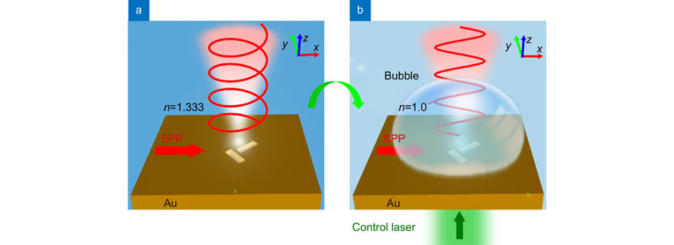
Fig. 1. (a ) Circularly polarized emission light as the plasmonic emitter is covered by water (n=1.333). (b ) Linearly polarized emission light as the plasmonic emitter is covered by a bubble (n=1.0) induced with a control laser beam.
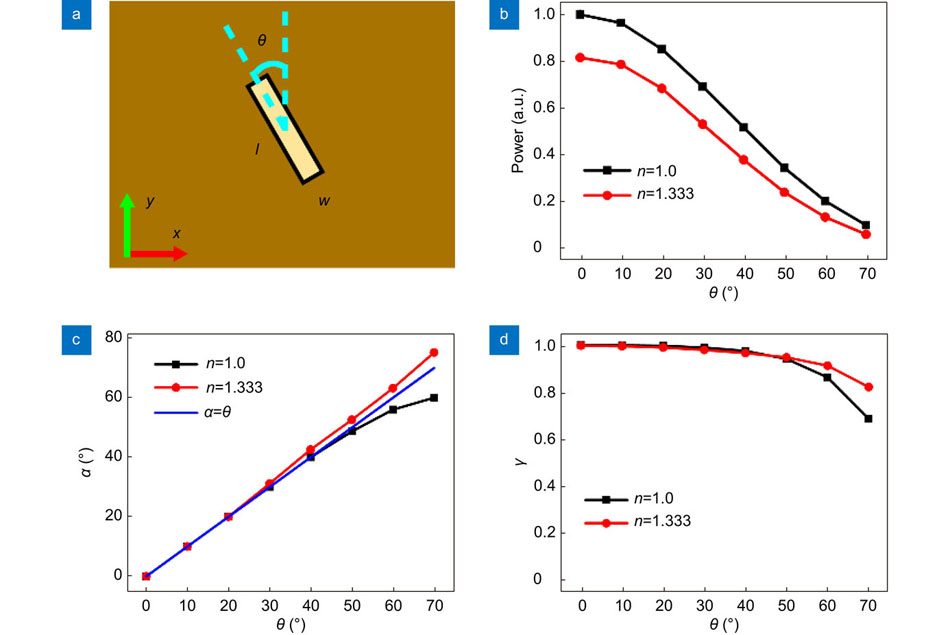
Fig. 2. (a ) Structure diagram and geometry parameters of a nanogroove antenna. Simulated (b ) powers, (c ) polarization orientation angles, and (d ) degrees of linear polarization (Dp) of the emission lights from one nanogroove antenna when the antenna is covered by different mediums with refractive indices of n=1.333 (red lines) and n=1.0 (black lines).
Fig. 3. (a ) Structure diagram and geometry parameters of the plasmonic emitter. (b ) Polar plot of the simulated intensity of the emission light from the plasmonic emitter as a function of the polarization angle for n=1.333 (red line) or n=1.0 (black line) at λ=900 nm. (c ) Degrees of linear polarization of the emission light from the plasmonic emitter varying with the wavelengths for n=1.333 (red line) or n=1.0 (black line).
Fig. 4. (a ) SEM image of the fabricated structure. (b ) Zoomed-in SEM image of a plasmonic emitter. (c ) Cross-section of a nanogroove antenna. The green lines is used to measure the thickness of the gold film and the depth of the nanogroove antenna. (d ) Schematic of the measurement set-up.
Fig. 5. (a ) Captured CMOS image of the sample in air. (b ) CMOS images of the emission light from the plasmonic emitter [denoted by the yellow dashed square in (a)] at different polarizer angles. (c ) Polar plot of the measured intensities of the emission light from the plasmonic emitter in air by rotating the polarizer. (d ) Captured CMOS image of the sample in water. (e ) CMOS images of the emission light from the plasmonic emitter [yellow dashed box in (d)] at different polarizer angles. (f ) Polar plot of the measured intensities of the emission light from the plasmonic emitter by rotating the polarizer at different pump intensities.
Fig. 6. (a ) CMOS image of a microbubble, which covers the sample. (b ) CMOS images of the emission light from the plasmonic emitter in the microbubble at different polarizer angles. (c ) Polar plot of the measured intensities of the emission light from the plasmonic emitter by rotating the polarizer in air (black), water (blue), and bubble (red). (d ) Polar plot of the simulated intensities of the emission light from the plasmonic emitter at different polarizer angles when the plasmonic emitter is covered by air (black), water (blue), and bubble (red). The result in air is the same as that in the bubble, so the red line is covered by the black line.


Set citation alerts for the article
Please enter your email address

© Copyright 2018-2021 | Chinese Laser Press. All Rights Reserved 沪ICP备15018463号-20